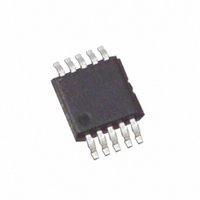
EL7532IYZ Intersil, EL7532IYZ Datasheet - Page 7

EL7532IYZ
Manufacturer Part Number
EL7532IYZ
Description
IC REG 2A STEP DOWN MONO 10MSOP
Manufacturer
Intersil
Type
Step-Down (Buck)r
Datasheet
1.EL7532IYZ.pdf
(8 pages)
Specifications of EL7532IYZ
Internal Switch(s)
Yes
Synchronous Rectifier
Yes
Number Of Outputs
1
Voltage - Output
0.8 ~ 5.5 V
Current - Output
2A
Frequency - Switching
1.5MHz
Voltage - Input
2.5 ~ 5.5 V
Operating Temperature
-40°C ~ 85°C
Mounting Type
Surface Mount
Package / Case
10-MSOP, Micro10™, 10-uMAX, 10-uSOP
Rohs Compliant
YES
Lead Free Status / RoHS Status
Lead free / RoHS Compliant
Power - Output
-
Available stocks
Company
Part Number
Manufacturer
Quantity
Price
Company:
Part Number:
EL7532IYZ
Manufacturer:
Intersil
Quantity:
308
Company:
Part Number:
EL7532IYZ
Manufacturer:
analogic
Quantity:
1 882
Part Number:
EL7532IYZ-T13
Manufacturer:
INTERSIL
Quantity:
20 000
Company:
Part Number:
EL7532IYZ-T7
Manufacturer:
Intersil
Quantity:
4 500
Part Number:
EL7532IYZ-T7
Manufacturer:
INT
Quantity:
20 000
recommended to be 22µF. Otherwise, if any of the above 3
conditions is not true, C
The RMS current present at the input capacitor is decided by
Equation 3:
This is about half of the output current I
input capacitor must be able to handle this current.
The inductor peak-to-peak ripple current is given as:
• L is the inductance
• f
The inductor must be able to handle I
current, and to assure that the inductor is reliable, it must
handle the 3A surge current that can occur during a current
limit condition.
In addition to decoupling capacitors and inductor value, it is
important to properly size the phase-lead capacitor C
(Refer to the Typical Application Diagram). The phase-lead
capacitor creates additional phase margin in the control loop
by generating a zero and a pole in the transfer function. As a
general rule of thumb, C
lead at a frequency of ~2.5kHz. The zero will always appear
at lower frequency than the pole and follow Equation 5:
Over a normal range of R
from ~470pF to 4700pF. The pole frequency cannot be set
once the zero frequency is chosen as it is dictated by the
ratio of R
output set point. Equation 6 shows the pole frequency
relationship:
f
f
ΔI
Z
P
I
INRMS
IL
S
=
=
the switching frequency (nominally 1.5MHz)
=
----------------------
2πR
---------------------------------------
2π R
(
------------------------------------------- -
(
V
1
1
=
2
IN
L
1
C
and R
----------------------------------------------- -
×
1
4
- V
R
V
V
O
2
IN
O
)C
×
×
2
)
(
V
4
, which is solely determined by the desired
×
f
V
S
IN
V
IN
O
- V
1
4
O
can remain as low as 10µF.
2
should be sized to start the phase-
)
(~10k to 100k), C
×
I
7
O
O
O
for the RMS load
for all the V
4
will range
O
4
(EQ. 3)
(EQ. 4)
(EQ. 5)
(EQ. 6)
. This
EL7532
Thermal Shut-Down
Once the junction reaches about +145°C, the regulator shuts
down. Both the P-Channel and the N-Channel MOSFETs
turn off. The output voltage will drop to zero. With the output
MOSFETs turned off, the regulator will soon cool down.
Once the junction temperature drops to about +130°C, the
regulator will restart again in the same manner as the EN pin
connects to logic HI.
Thermal Performance
The EL7532 is in a fused-lead MSOP10 package. Compared
to the regular MSOP10 package, the fused-lead package
provides lower thermal resistance. The typical θ
+115°C/W (See Thermal Information section in spec table)
can be improved by maximizing the copper area around the
pins. A θ
and +125°C/W on a 2-layer board. Refer to Intersil’s Tech
Brief, TB379, for more information on thermal resistance.
Layout Considerations
The layout is very important for the converter to function
properly. The following PC layout guidelines should be
followed:
• Separate the Power Ground ( ) and Signal Ground ( );
• Place the input capacitor as close to V
• Make the following PC traces as small as possible:
• If used, connect the trace from the FB pin to R
• Maximize the copper area around the PGND pin
• Place several via holes under the chip to additional ground
The demo board is a good example of layout based on this
outline. Please refer to the EL7532 Application Brief.
connect them only at one point right at the pins
as possible
- from L
- from C
close as possible
plane to improve heat dissipation
JA
X
O
of +100°C/W can be achieved on a 4-layer board
pin to L
to PGND
IN
and PGND pins
November 2, 2007
JA
1
and R
of
FN7435.8
2
as


