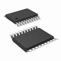
LM20343MH/NOPB National Semiconductor, LM20343MH/NOPB Datasheet - Page 15

LM20343MH/NOPB
Manufacturer Part Number
LM20343MH/NOPB
Description
IC REG SYNC BUCK 3A 20TSSOP
Manufacturer
National Semiconductor
Series
PowerWise®r
Type
Step-Down (Buck)r
Datasheet
1.LM20343MHNOPB.pdf
(20 pages)
Specifications of LM20343MH/NOPB
Internal Switch(s)
Yes
Synchronous Rectifier
Yes
Number Of Outputs
1
Voltage - Output
0.8 ~ 32 V
Current - Output
3A
Frequency - Switching
250kHz, 750kHz
Voltage - Input
4.5 ~ 36 V
Operating Temperature
-40°C ~ 125°C
Mounting Type
Surface Mount
Package / Case
20-TSSOP Exposed Pad, 20-eTSSOP, 20-HTSSOP
Primary Input Voltage
36V
No. Of Outputs
1
Output Voltage
32V
Output Current
3A
No. Of Pins
20
Operating Temperature Range
-40°C To +125°C
Msl
MSL 1 - Unlimited
Filter Terminals
SMD
Rohs Compliant
Yes
For Use With
LM20343EVAL - EVALUATION BOARD FOR THE LM20343
Lead Free Status / RoHS Status
Lead free / RoHS Compliant
Power - Output
-
Other names
*LM20343MH
*LM20343MH/NOPB
LM20343MH
*LM20343MH/NOPB
LM20343MH
Similar to the soft-start function, the fastest start up possible
is 1ms regardless of the rise time of the tracking voltage.
When using the track feature the final voltage seen by the SS/
TRACK pin should exceed 1V to provide sufficient overdrive
and transient immunity.
BENEFIT OF AN EXTERNAL SCHOTTKY
The LM20343 employs a 40ns dead time between conduction
of the control and synchronous FETs in order to avoid the
situation where both FETs simultaneously conduct, causing
shoot-through current. During the dead time, the body diode
of the synchronous FET acts as a free-wheeling diode and
conducts the inductor current. The structure of the high volt-
age DMOS is optimized for high breakdown voltage, but this
typically leads to inefficient body diode conduction due to the
reverse recovery charge. The loss associated with the re-
verse recovery of the body diode of the synchronous FET
manifests itself as a loss proportional to load current and
switching frequency. The additional efficiency loss becomes
apparent at higher input voltages and switching frequencies.
One simple solution is to use a small 1A external Schottky
diode between SW and GND as shown in Figure 14. The ex-
ternal Schottky diode effectively conducts all inductor current
during the dead time, minimizing the current passing through
the synchronous MOSFET body diode and eliminating re-
verse recovery losses.
The external Schottky conducts currents for a very small por-
tion of the switching cycle, therefore the average current is
low. An external Schottky rated for 1A will improve efficiency
by several percent in some applications. A Schottky rated at
a higher current will not significantly improve efficiency and
may be worse due to the increased reverse capacitance. The
forward voltage of the synchronous MOSFET body diode is
approximately 700 mV, therefore an external Schottky with a
forward voltage less than or equal to 700 mV should be se-
lected to ensure the majority of the dead time current is carried
by the Schottky.
THERMAL CONSIDERATIONS
The thermal characteristics of the LM20343 are specified us-
ing the parameter θ
to the ambient temperature. Although the value of θ
pendant on many variables, it still can be used to approximate
the operating junction temperature of the device.
To obtain an estimate of the device junction temperature, one
may use the following relationship:
and
Where:
T
P
θ
LM20343.
T
I
DCR is the inductor series resistance.
It is important to always keep the operating junction temper-
ature (T
temperature exceeds 170°C the device will cycle in and out
of thermal shutdown. If thermal shutdown occurs it is a sign
of inadequate heatsinking or excessive power dissipation in
the device.
OUT
J
JA
A
IN
is the junction temperature in °C.
is the ambient temperature in °C.
is the input power in Watts (P
is the junction to ambient thermal resistance for the
is the output load current.
P
J
D
) below 125°C for reliable operation. If the junction
= P
IN
x (1 - Efficiency) - 1.1 x (I
JA
T
, which relates the junction temperature
J
= P
D
x θ
JA
IN
+ T
= V
A
IN
OUT
x I
IN
)
2
).
x DCR
JA
is de-
15
Figure 8, Figure 9, Figure 10 and Figure 11 can be used as a
guide to avoid exceeding the maximum junction temperature
of 125°C provided an external 1A Schottky diode, such as
Central Semiconductor's CMMSH1-40-NST, is used to im-
prove reverse recovery losses.
FIGURE 8. Safe Thermal Operating Areas (I
FIGURE 9. Safe Thermal Operating Areas (I
= 500 kHz)
= 350kHz)
OUT
OUT
30051790
30051788
www.national.com
= 3A, f
= 3A, f
SW
SW


