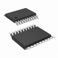
LM20343MH/NOPB National Semiconductor, LM20343MH/NOPB Datasheet - Page 3

LM20343MH/NOPB
Manufacturer Part Number
LM20343MH/NOPB
Description
IC REG SYNC BUCK 3A 20TSSOP
Manufacturer
National Semiconductor
Series
PowerWise®r
Type
Step-Down (Buck)r
Datasheet
1.LM20343MHNOPB.pdf
(20 pages)
Specifications of LM20343MH/NOPB
Internal Switch(s)
Yes
Synchronous Rectifier
Yes
Number Of Outputs
1
Voltage - Output
0.8 ~ 32 V
Current - Output
3A
Frequency - Switching
250kHz, 750kHz
Voltage - Input
4.5 ~ 36 V
Operating Temperature
-40°C ~ 125°C
Mounting Type
Surface Mount
Package / Case
20-TSSOP Exposed Pad, 20-eTSSOP, 20-HTSSOP
Primary Input Voltage
36V
No. Of Outputs
1
Output Voltage
32V
Output Current
3A
No. Of Pins
20
Operating Temperature Range
-40°C To +125°C
Msl
MSL 1 - Unlimited
Filter Terminals
SMD
Rohs Compliant
Yes
For Use With
LM20343EVAL - EVALUATION BOARD FOR THE LM20343
Lead Free Status / RoHS Status
Lead free / RoHS Compliant
Power - Output
-
Other names
*LM20343MH
*LM20343MH/NOPB
LM20343MH
*LM20343MH/NOPB
LM20343MH
Powergood
Oscillator
Error Amplifier
V
R
R
I
V
I
Absolute Maximum Ratings
If Military/Aerospace specified devices are required,
please contact the National Semiconductor Sales Office/
Distributors for availability and specifications.
Electrical Characteristics
type are for T
and Maximum limits are guaranteed through test, design, or statistical correlation. Typical values represent the most likely
parametric norm at T
V
I
VIN to GND
BOOT to GND
BOOT to SW
SW to GND
SW to GND (Transient)
FB, EN, SS/TRK, RT,
PGOOD to GND
PGOOD(SNK)
PGOOD(SRC)
I
FB(OVP-HYS)
COMP(SRC)
HSW-DS(ON)
COMP(SNK)
Symbol
LSW-DS(ON)
V
V
FB(PG-HYS)
V
UVLO(HYS)
T
V
V
GBW
TRKACC
I
FB(OVP)
D
V
PGOOD
F
F
A
F-BOOT
BOOT
FB(PG)
V
V
I
UVLO
I
I
g
I
VCC
SW1
SW2
MAX
SD
SS
VOL
FB
Q
RT
FB
m
J
Parameter
Feedback Pin Voltage
High-Side MOSFET On-Resistance
Low-Side MOSFET On-Resistance
Operating Quiescent Current
Shutdown Quiescent Current
VIN Under Voltage Lockout
VIN Under Voltage Lockout Hysteresis
VCC Voltage
Soft-Start Pin Source Current
Soft-Start/Track Pin Accuracy
BOOT Diode Leakage
BOOT Diode Forward Voltage
Over Voltage Protection Rising Threshold
Over Voltage Protection Hysteresis
PGOOD Threshold, V
PGOOD Hysteresis
PGOOD Delay
PGOOD Low Sink Current
PGOOD High Leakage Current
Switching Frequency 1
Switching Frequency 2
Maximum Duty Cycle
RT pin voltage
Feedback Pin Bias Current
COMP Output Source Current
COMP Output Sink Current
Error Amplifier DC Transconductance
Error Amplifier Voltage Gain
Error Amplifier Gain-Bandwidth Product
= 25°C only, limits in bold face type apply over the junction temperature (T
J
= 25°C, and are provided for reference purposes only.
OUT
Rising
-1.5V (< 20 ns)
Unless otherwise stated, the following conditions apply: V
-0.3V to +38V
-0.3V to +43V
-0.5V to +38V
-0.3V to +7V
-0.3V to +6V
(Note 1)
3
Conditions
V
I
I
V
V
Rising V
I
V
V
V
I
V
Δ
V
ΔV
V
V
R
R
I
R
V
V
V
V
V
I
COMP pin open
COMP pin open
SW
SW
VCC
BOOT
LOAD
COMP
VIN
VIN
EN
SS
SS
BOOT
FB(OVP)
VFB(OVP)
FB(PG)
PGOOD
PGOOD
RT
RT
RT
FB
FB
COMP
FB
COMP
VIN to GND
Junction Temperature
Operating Ratings
FB(PG)
VCC to GND
Storage Temperature
ESD Rating
Human Body Model (Note 2)
= 3A
= 3A
= 1V
= 0V
= 1.6V
= 0V
= 0V
= 0.4V
= 49.9 kΩ
= 249 kΩ
= 249 kΩ
= -5 mA, V
= 4.5V to 36V
= 4.5V to 36V
= 3A
= -100 mA
= -50 µA to +50 µA
= 4V
= 0V
= 1.6V
/ V
= 0.5V
= 5V
VIN
/ V
/ V
/ V
FB
FB
FB
FB
EN
= 5V
J
) range of -40°C to +125°C. Minimum
0.788
VIN
Min
107
675
225
200
200
450
-10
0.6
93
4
2
= 12V. Limits in standard
2000
4.25
Typ
130
110
150
350
110
750
250
550
400
350
515
0.8
2.3
5.5
0.9
10
95
20
80
50
−40°C to + 125°C
5
5
2
2
1
5
7
-65°C to 150°C
+4.5V to +36V
-0.3V to +8V
www.national.com
0.812
Max
225
190
180
450
112
200
825
325
600
4.5
1.1
15
97
3
7
3
3
2kV
Units
µmho
MHz
kHz
kHz
mΩ
mΩ
V/V
mA
mV
mV
mA
mV
µA
µA
nA
nA
nA
µA
µA
µs
%
%
%
%
%
V
V
V
V


