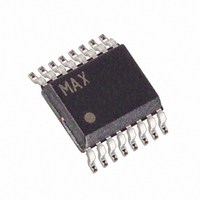
MAX8543EEE+ Maxim Integrated Products, MAX8543EEE+ Datasheet - Page 18

MAX8543EEE+
Manufacturer Part Number
MAX8543EEE+
Description
IC CNTRLR STEP DOWN 16-QSOP
Manufacturer
Maxim Integrated Products
Type
Step-Down (Buck)r
Datasheet
1.MAX8543EEE.pdf
(27 pages)
Specifications of MAX8543EEE+
Internal Switch(s)
No
Synchronous Rectifier
No
Number Of Outputs
1
Voltage - Output
0.8 ~ 11 V
Current - Output
25A
Frequency - Switching
200kHz ~ 1MHz
Voltage - Input
3 ~ 13.2 V
Operating Temperature
-40°C ~ 85°C
Mounting Type
Surface Mount
Package / Case
16-QSOP
Power - Output
667mW
Output Voltage
0.8 V to 11.88 V
Output Current
25000 mA
Mounting Style
SMD/SMT
Switching Frequency
200 KHz to 1000 KHz
Maximum Operating Temperature
+ 85 C
Minimum Operating Temperature
- 40 C
Synchronous Pin
Yes
Topology
Buck
Lead Free Status / RoHS Status
Lead free / RoHS Compliant
Step-Down Controllers with Prebias Startup,
Lossless Sensing, Synchronization, and OVP
Figure 4. Inductor-Current Waveform
The MAX8543/MAX8544 have an adjustable internal
oscillator that can be set to any frequency from 200kHz
to 1MHz. To set the switching frequency, connect a
resistor from FSYNC to GND. Calculate the resistor
value from the following equation:
The MAX8543/MAX8544 can also be synchronized to an
external clock by connecting the clock signal to FSYNC.
When using an external clock, select R
the free-running frequency is within ±30% of the clock fre-
quency. In addition, the MAX8544 has a synchronization
output (SYNCO) that provides a clock signal that is 180°
out-of-phase with the MAX8544 switching. SYNCO is
used to synchronize a second controller 180° out-of-
phase with the first by connecting SYNCO of the first con-
troller to FSYNC of the second when the first controller
operates in free-running mode. When the first controller is
synchronized to an external clock, the external clock is
inverted to generate SYNCO.
POK is an open-drain output on the MAX8544 that moni-
tors the output voltage. When the output is above 91% of
its nominal regulation voltage, POK is high impedance.
When the output drops below 91% of its nominal regula-
tion voltage, POK is pulled low. POK is also pulled low
when the MAX8544 is shut down. To use POK as a logic-
level signal, connect a pullup resistor from POK to the
logic-supply rail.
18
______________________________________________________________________________________
R
FSYNC
=
⎛
⎜
⎝
2
Switching Frequency and
Power-Good Signal (POK)
1
f
S
−
240
ns
TIME
⎞
⎟
⎠
⎛
⎜
⎝
Synchronization
14 18
1
.
k
FSYNC
Ω
ns
⎞
⎟
⎠
I
I
I
PEAK
LOAD
VALLEY
such that
Thermal-overload protection limits total power dissipation
in the MAX8543/MAX8544. When the junction tempera-
ture exceeds T
shuts down the device, allowing the IC to cool. The ther-
mal sensor turns the IC on again after the junction tem-
perature cools by 15°C, resulting in a pulsed output
during continuous thermal-overload conditions.
To set the output voltage for the MAX8543/MAX8544,
connect FB to the center of an external resistor-divider
from the output to GND (Figure 5). Select R2 between
8kΩ and 24kΩ; then calculate R1 with the following
equation:
where V
close to the IC as possible.
There are several parameters that must be examined
when determining which inductor is to be used: input volt-
age, output voltage, load current, switching frequency,
and LIR. LIR is the ratio of peak-to peak inductor current
ripple to maximum DC load current. A higher LIR value
allows for a smaller inductor, but results in higher losses
and higher output ripple.
Figure 5. Setting the Output Voltage with a Resistor Voltage-
Divider
FB
MAX8543/
MAX8544
= 0.8V. R1 and R2 should be placed as
J
= +160°C, an internal thermal sensor
R
Thermal-Overload Protection
1
=
Setting the Output Voltage
R
LX
FB
2
×
⎛
⎜
⎝
Design Procedure
V
V
OUT
FB
Inductor Selection
−
1
⎞
⎟
⎠
R1
R2


