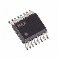
MAX8543EEE+ Maxim Integrated Products, MAX8543EEE+ Datasheet - Page 22

MAX8543EEE+
Manufacturer Part Number
MAX8543EEE+
Description
IC CNTRLR STEP DOWN 16-QSOP
Manufacturer
Maxim Integrated Products
Type
Step-Down (Buck)r
Datasheet
1.MAX8543EEE.pdf
(27 pages)
Specifications of MAX8543EEE+
Internal Switch(s)
No
Synchronous Rectifier
No
Number Of Outputs
1
Voltage - Output
0.8 ~ 11 V
Current - Output
25A
Frequency - Switching
200kHz ~ 1MHz
Voltage - Input
3 ~ 13.2 V
Operating Temperature
-40°C ~ 85°C
Mounting Type
Surface Mount
Package / Case
16-QSOP
Power - Output
667mW
Output Voltage
0.8 V to 11.88 V
Output Current
25000 mA
Mounting Style
SMD/SMT
Switching Frequency
200 KHz to 1000 KHz
Maximum Operating Temperature
+ 85 C
Minimum Operating Temperature
- 40 C
Synchronous Pin
Yes
Topology
Buck
Lead Free Status / RoHS Status
Lead free / RoHS Compliant
Step-Down Controllers with Prebias Startup,
Lossless Sensing, Synchronization, and OVP
Fast switching transitions cause ringing because of res-
onating circuit parasitic inductance and capacitance at
the switching nodes. This high-frequency ringing
occurs at LX’s rising and falling transitions and can
interfere with circuit performance and generate EMI. To
dampen this ringing, a series RC snubber circuit is
added across each switch. Below is the procedure for
selecting the value of the series RC circuit.
Connect a scope probe to measure V
observe the ringing frequency, f
Find the capacitor value (connected from LX to GND)
that reduces the ringing frequency by half.
The circuit parasitic capacitance (C
equal to 1/3rd the value of the added capacitance above.
The circuit parasitic inductance (L
The resistor for critical dampening (R
2π x f
to tailor the desired damping and the peak voltage
excursion.
The capacitor (C
value of the C
snubber circuit (P
can be calculated as:
where V
frequency. Choose an R
the specific application’s derating rule for the power
dissipation calculated.
The input filter capacitor reduces peak currents drawn
from the power source and reduces noise and voltage
ripple on the input caused by the circuit’s switching.
The input capacitor must meet the ripple-current
requirement (I
defined by the following equation:
22
______________________________________________________________________________________
R
IN
x L
I
RMS
is the input voltage and f
P
PAR
RSNUB
PAR
RMS
=
L
. Adjust the resistor value up or down
SNUB
PAR
I
RSNUB
LOAD
to be effective. The power loss of the
) imposed by the switching currents
=
=
) should be at least 2 to 4 times the
C
(
SNUB
MOSFET Snubber Circuit
) is dissipated in the resistor and
2
V
SNUB
π
OUT
f
R
)
V
2
×
IN
×
1
( )
power rating that meets
×
R
V
(
PAR
.
IN
V
C
IN
PAR
Input Capacitor
2
SW
) is calculated by:
−
PAR
SNUB
×
V
OUT
f
LX
is the switching
SW
) at LX is then
to GND and
) is equal to
)
I
twice the output voltage (V
I
their low ESR and ESL at high frequency with relatively
low cost. Choose a capacitor that exhibits less than 10°C
temperature rise at the maximum operating RMS current
for optimum long-term reliability. Ceramic capacitors with
an X5R or better temperature characteristic are recom-
mended. When operating from a soft input source, an
additional input capacitor (bulk bypass capacitor) may
be required to prevent input from sagging.
The key selection parameters for the output capacitor
are the actual capacitance value, the equivalent series
resistance (ESR), the equivalent series inductance
(ESL), and the voltage-rating requirements. These
parameters affect the overall stability, output voltage
ripple, and transient response. The output ripple has
three components: variations in the charge stored in
the output capacitor, the voltage drop across the
capacitor’s ESR, and ESL caused by the current into
and out of the capacitor. The maximum output voltage
ripple is estimated as follows:
The output voltage ripple as a consequence of the
ESR, ESL, and output capacitance is:
where I
These equations are suitable for initial capacitor selec-
tion, but final values should be chosen based on a proto-
type or evaluation circuit. As a general rule, a smaller
current ripple results in less output voltage ripple. Since
the inductor ripple current is a factor of the inductor value
and input voltage, the output voltage ripple decreases
with larger inductance, and increases with higher input
voltages. Polymer, tantalum, or aluminum electrolytic
capacitors are recommended.
RMS
LOAD
V
RIPPLE
has a maximum value when the input voltage equals
/ 2. Ceramic capacitors are recommended due to
P-P
= V
is the peak-to-peak inductor current:
RIPPLE(ESR)
I
V
V
P P
V
RIPPLE C
RIPPLE ESR
−
RIPPLE ESL
=
V
( )
(
IN
(
f
S
−
=
IN
+ V
)
×
)
V
8
=
OUT
= 2 x V
L
=
×
RIPPLE(C)
I
P P
V
C
−
IN
L
I
P P
OUT
×
Output Capacitor
−
×
×
OUT
V
ESL
ESR
OUT
V
×
IN
f
), so I
S
+ V
RIPPLE(ESL)
RMS(MAX)
=


