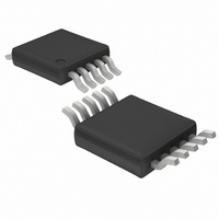
LTC1871IMS-1#TRPBF Linear Technology, LTC1871IMS-1#TRPBF Datasheet - Page 14

LTC1871IMS-1#TRPBF
Manufacturer Part Number
LTC1871IMS-1#TRPBF
Description
IC CONTRLR CURRENT MODE 10-MSOP
Manufacturer
Linear Technology
Type
Step-Up (Boost), Flyback, Sepicr
Datasheet
1.LTC1871EMS-1PBF.pdf
(36 pages)
Specifications of LTC1871IMS-1#TRPBF
Internal Switch(s)
No
Synchronous Rectifier
No
Number Of Outputs
1
Voltage - Output
1.23 ~ 72 V
Current - Output
50mA
Frequency - Switching
50kHz ~ 1MHz
Voltage - Input
2.5 ~ 36 V
Operating Temperature
-40°C ~ 125°C
Mounting Type
Surface Mount
Package / Case
10-MSOP, Micro10™, 10-uMAX, 10-uSOP
Lead Free Status / RoHS Status
Lead free / RoHS Compliant
Power - Output
-
Available stocks
Company
Part Number
Manufacturer
Quantity
Price
LTC1871-1
APPLICATIONS INFORMATION
Remember that boost converters are not short-circuit
protected. Under a shorted output condition, the inductor
current is limited only by the input supply capability. For
applications requiring a step-up converter that is short-
circuit protected, please refer to the applications section
covering SEPIC converters.
The minimum required saturation current of the inductor
can be expressed as a function of the duty cycle and the
load current, as follows:
The saturation current rating for the inductor should be
checked at the minimum input voltage (which results
in the highest inductor current) and maximum output
current.
Boost Converter: Operating in Discontinuous Mode
Discontinuous mode operation occurs when the load cur-
rent is low enough to allow the inductor current to run out
during the off-time of the switch, as shown in Figure 9.
Once the inductor current is near zero, the switch and diode
capacitances resonate with the inductance to form damped
ringing at 1MHz to 10MHz. If the off-time is long enough,
the drain voltage will settle to the input voltage.
Depending on the input voltage and the residual energy
in the inductor, this ringing can cause the drain of the
power MOSFET to go below ground where it is clamped
by the body diode. This ringing is not harmful to the IC
and it has not been shown to contribute signifi cantly to
EMI. Any attempt to damp it with a snubber will degrade
the effi ciency.
14
MOSFET DRAIN
I
L(SAT)
INDUCTOR
CURRENT
VOLTAGE
2V/DIV
2A/DIV
Figure 9. Discontinuous Mode Waveforms
V
V
1+
IN
OUT
= 3.3V I
= 5V
2
OUT
•
1– D
I
= 200mA
O(MAX)
2μs/DIV
MAX
18711 F09
Boost Converter: Inductor Core Selection
Once the value for L is known, the type of inductor must
be selected. High effi ciency converters generally cannot
afford the core loss found in low cost powdered iron cores,
forcing the use of more expensive ferrite, molypermalloy
or Kool Mμ
size for a fi xed inductor value, but is very dependent on
the inductance selected. As inductance increases, core
losses go down. Unfortunately, increased inductance
requires more turns of wire and therefore, copper losses
will increase. Generally, there is a tradeoff between core
losses and copper losses that needs to be balanced.
Ferrite designs have very low core losses and are pre-
ferred at high switching frequencies, so design goals can
concentrate on copper losses and preventing saturation.
Ferrite core material saturates “hard,” meaning that the
inductance collapses rapidly when the peak design current
is exceeded. This results in an abrupt increase in inductor
ripple current and consequently, output voltage ripple. Do
not allow the core to saturate!
Molypermalloy (from Magnetics, Inc.) is a very good,
low cost core material for toroids, but is more expensive
than ferrite. A reasonable compromise from the same
manufacturer is Kool Mμ.
Boost Converter: Power MOSFET Selection
The power MOSFET serves two purposes in the LTC1871-1:
it represents the main switching element in the power path,
and its R
for the control loop. Important parameters for the power
MOSFET include the drain-to-source breakdown voltage
(BV
(R
and gate-to-drain charges (Q
the maximum drain current (I
thermal resistances (R
The gate drive voltage is set by the 5.2V INTV
regulator. Consequently, logic-level threshold MOSFETs
should be used in most LTC1871-1 applications. If low
input voltage operation is expected (e.g., supplying power
DS(ON)
DSS
), the threshold voltage (V
) versus gate-to-source voltage, the gate-to-source
DS(ON)
®
cores. Actual core loss is independent of core
represents the current sensing element
TH(JC)
and R
GS
D(MAX)
GS(TH)
and Q
TH(JA)
) and the MOSFET’s
), the on-resistance
GD
).
, respectively),
CC
low drop
18711fb


