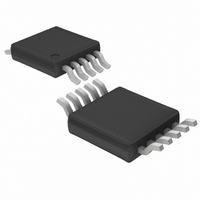
LTC1871IMS-1#TRPBF Linear Technology, LTC1871IMS-1#TRPBF Datasheet - Page 4

LTC1871IMS-1#TRPBF
Manufacturer Part Number
LTC1871IMS-1#TRPBF
Description
IC CONTRLR CURRENT MODE 10-MSOP
Manufacturer
Linear Technology
Type
Step-Up (Boost), Flyback, Sepicr
Datasheet
1.LTC1871EMS-1PBF.pdf
(36 pages)
Specifications of LTC1871IMS-1#TRPBF
Internal Switch(s)
No
Synchronous Rectifier
No
Number Of Outputs
1
Voltage - Output
1.23 ~ 72 V
Current - Output
50mA
Frequency - Switching
50kHz ~ 1MHz
Voltage - Input
2.5 ~ 36 V
Operating Temperature
-40°C ~ 125°C
Mounting Type
Surface Mount
Package / Case
10-MSOP, Micro10™, 10-uMAX, 10-uSOP
Lead Free Status / RoHS Status
Lead free / RoHS Compliant
Power - Output
-
Available stocks
Company
Part Number
Manufacturer
Quantity
Price
ELECTRICAL CHARACTERISTICS
LTC1871-1
temperature range, otherwise specifi cations are at T
SYMBOL
Low Dropout Regulator
V
ΔV
ΔV
V
V
I
GATE Driver
t
t
Note 1: Stresses beyond those listed under Absolute Maximum Ratings
may cause permanent damage to the device. Exposure to any Absolute
Maximum Rating condition for extended periods may affect device
reliability and lifetime.
Note 2: The LTC1871E-1 is guaranteed to meet performance specifi cations
from 0°C to 85°C junction temperature. Specifi cations over the – 40°C
to 85°C operating junction temperature range are assured by design,
characterization and correlation with statistical process controls. The
LTC1871I-1 is guaranteed over the full –40°C to 125°C operating junction
temperature range.
Note 3: T
dissipation P
TYPICAL PERFORMANCE CHARACTERISTICS
4
INTVCC
r
f
INTVCC
ΔV
LDO(LOAD)
DROPOUT
ΔV
INTVCC
INTVCC
T
1.25
1.24
1.23
1.22
1.21
IN1
IN2
J
= T
–50
FB Voltage vs Temp
J
A
is calculated from the ambient temperature T
+ (P
–25
D
PARAMETER
INTV
INTV
INTV
INTV
INTV
Bootstrap Mode INTV
GATE Driver Output Rise Time
GATE Driver Output Fall Time
according to the following formula:
D
• 110°C/W)
0
CC
CC
CC
CC
CC
TEMPERATURE (°C)
25
Regulator Output Voltage
Regulator Line Regulation
Regulator Line Regulation
Load Regulation
Regulator Dropout Voltage
50
75
CC
100
Supply
125
18711 G01
150
A
1.231
1.230
1.229
A
and power
= 25°C. V
CONDITIONS
V
V
7.5V ≤ V
15V ≤ V
0 ≤ I
INTV
RUN = 0V, SENSE = 5V
I-Grade (Note 2)
C
C
FB Voltage Line Regulation
0
IN
IN
L
L
= 3300pF (Note 7)
= 3300pF (Note 7)
= 7.5V
= 7.5V, I-Grade (Note 2)
INTVCC
CC
5
The
Load = 20mA
IN
IN
IN
≤ 30V
= 5V, V
≤ 15V
10
≤ 20mA, V
l
denotes the specifi cations which apply over the full operating
15
V
RUN
IN
Note 4: The dynamic input supply current is higher due to power MOSFET
gate charging (Q
Note 5: The LTC1871-1 is tested in a feedback loop which servos V
the reference voltage with the I
range (0.3V ≤ V
Note 6: In a synchronized application, the internal slope compensation
gain is increased by 25%. Synchronizing to a signifi cantly higher ratio will
reduce the effective amount of slope compensation, which could result in
subharmonic oscillation for duty cycles greater than 50%.
Note 7: Rise and fall times are measured at 10% and 90% levels.
(V)
IN
20
= 1.5V, R
= 7.5V
25
FREQ
30
18711 G02
ITH
G
= 80k, V
• f
≤ 1.2V, midpoint = 0.75V).
35
OSC
). See Applications Information.
MODE/SYNC
60
50
40
30
20
10
TH
●
●
0
–50
pin forced to the midpoint of its voltage
FB Pin Current vs Temperature
–25
MIN
5.0
5.0
– 2
= 0V, unless otherwise specifi ed.
0
TEMPERATURE (°C)
–0.2
TYP
280
25
5.2
5.2
70
10
17
8
8
50
MAX
200
100
100
75
5.4
5.4
25
20
30
100
125 150
FB
18711 G03
UNITS
18711fb
to
mV
mV
mV
μA
μA
ns
ns
%
V
V


