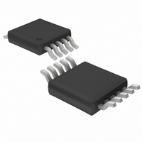
LTC1871IMS-1#TRPBF Linear Technology, LTC1871IMS-1#TRPBF Datasheet - Page 21

LTC1871IMS-1#TRPBF
Manufacturer Part Number
LTC1871IMS-1#TRPBF
Description
IC CONTRLR CURRENT MODE 10-MSOP
Manufacturer
Linear Technology
Type
Step-Up (Boost), Flyback, Sepicr
Datasheet
1.LTC1871EMS-1PBF.pdf
(36 pages)
Specifications of LTC1871IMS-1#TRPBF
Internal Switch(s)
No
Synchronous Rectifier
No
Number Of Outputs
1
Voltage - Output
1.23 ~ 72 V
Current - Output
50mA
Frequency - Switching
50kHz ~ 1MHz
Voltage - Input
2.5 ~ 36 V
Operating Temperature
-40°C ~ 125°C
Mounting Type
Surface Mount
Package / Case
10-MSOP, Micro10™, 10-uMAX, 10-uSOP
Lead Free Status / RoHS Status
Lead free / RoHS Compliant
Power - Output
-
Available stocks
Company
Part Number
Manufacturer
Quantity
Price
APPLICATIONS INFORMATION
5. With the input voltage to the IC bootstrapped to the
6. The diode for this design must handle a maximum
7. The output capacitor usually consists of a high valued
The inductor ripple current is:
And so the inductor value is:
The component chosen is a 1μH inductor made by
Sumida (part number CEP125-H 1ROMH) which has
a saturation current of greater than 20A.
output of the power supply (5V), a logic-level MOSFET
can be used. Because the duty cycle is 39%, the maxi-
mum SENSE pin threshold voltage is reduced from its
low duty cycle typical value of 150mV to approximately
140mV. Assuming a MOSFET junction temperature of
125°C, the room temperature MOSFET R
be less than:
The MOSFET used was the Fairchild FDS7760A, which
has a maximum R
of greater than 30V, and a gate charge of 37nC at 5V
V
DC output current of 10A and be rated for a minimum
reverse voltage of V
On Semiconductor (MBRB2515L) was chosen for its
high power dissipation capability.
bulk C connected in parallel with a lower valued, low
L =
GS
I
L
R
= 0.140V •
.
V
= •
DS(ON)
IN(MIN)
I
L
• f
1– D
I
O(MAX)
• D
V
MAX
SENSE(MAX)
MAX
1+
DS(ON)
= 0.4 •
0.4
OUT
=
1– 0.39
2
4.6A • 300kHz
, or 5V. A 25A, 15V diode from
• 7A • 1.5
of 8mΩ at 4.5V V
1– 0.39
•
3.3V
1+
7
2
1– D
= 6.8m
= 4.6A
•I
• 0.39 = 0.93μH
O(MAX)
MAX
DS(ON)
GS
, a BV
•
should
T
DSS
8. The choice of an input capacitor for a boost converter
ESR ceramic. Based on a maximum output ripple voltage
of 1%, or 50mV, the bulk C needs to be greater than:
The RMS ripple current rating for this capacitor needs
to exceed:
To satisfy this high RMS current demand, four 150μF
Panasonic capacitors (EEFUEOJ151R) are required.
In parallel with these bulk capacitors, two 22μF , low
ESR (X5R) Taiyo Yuden ceramic capacitors (JMK-
325BJ226MM) are added for HF noise reduction.
Check the output ripple with a single oscilloscope
probe connected directly across the output capacitor
terminals, where the HF switching currents fl ow.
depends on the impedance of the source supply and the
amount of input ripple the converter will safely toler-
ate. For this particular design and lab setup a 100μF
Sanyo Poscap (6TPC 100M), in parallel with two 22μF
Taiyo Yuden ceramic capacitors (JMK325BJ226MM)
is required (the input and return lead lengths are kept
to a few inches, but the peak input current is close to
20A!). As with the output node, check the input ripple
with a single oscilloscope probe connected across the
input capacitor terminals.
I
C
7A •
0.01• 5V • 300kHz
RMS(COUT)
OUT
5V – 3.3V
0.01• V
7A
I
3.3V
OUT(MAX)
I
O(MAX)
OUT
= 5A
= 466μF
• f
•
=
V
O
V
– V
IN(MIN)
LTC1871-1
IN(MIN)
=
21
18711fb


