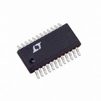
LTC3713EG Linear Technology, LTC3713EG Datasheet - Page 14

LTC3713EG
Manufacturer Part Number
LTC3713EG
Description
IC DC/DC CONTROLLER SYNC 24-SSOP
Manufacturer
Linear Technology
Type
Step-Down (Buck)r
Datasheet
1.LTC3713EGPBF.pdf
(24 pages)
Specifications of LTC3713EG
Internal Switch(s)
No
Synchronous Rectifier
Yes
Number Of Outputs
1
Voltage - Output
0.8 ~ 32.4 V
Current - Output
2A
Voltage - Input
1.5 ~ 36 V
Operating Temperature
-40°C ~ 85°C
Mounting Type
Surface Mount
Package / Case
24-SSOP
Lead Free Status / RoHS Status
Contains lead / RoHS non-compliant
Power - Output
-
Frequency - Switching
-
Available stocks
Company
Part Number
Manufacturer
Quantity
Price
Company:
Part Number:
LTC3713EG
Manufacturer:
LINEAR
Quantity:
208
Part Number:
LTC3713EG
Manufacturer:
LINEAR/凌特
Quantity:
20 000
Part Number:
LTC3713EG#PBF
Manufacturer:
LINEAR/凌特
Quantity:
20 000
Part Number:
LTC3713EG#TRPBF
Manufacturer:
LINEAR/凌特
Quantity:
20 000
APPLICATIO S I FOR ATIO
LTC3713
Tantalum capacitors have the highest capacitance density
but it is important to only use types that have been surge
tested for use in switching power supplies. Aluminum
electrolytic capacitors have significantly higher ESR, but
can be used in cost-sensitive applications providing that
consideration is given to ripple current ratings and long
term reliability. Ceramic capacitors have excellent low
ESR characteristics but can have a high voltage coeffi-
cient and audible piezoelectric effects. The high Q of
ceramic capacitors with trace inductance can also lead to
significant ringing. When used as input capacitors, care
must be taken to ensure that ringing from inrush currents
and switching does not pose an overvoltage hazard to the
power switches and controller. To dampen input voltage
transients, add a small 5 F to 50 F aluminum electrolytic
capacitor with an ESR in the range of 0.5 to 2 . High
performance through-hole capacitors may also be used,
but an additional ceramic capacitor in parallel is recom-
mended to reduce the effect of their lead inductance.
Top MOSFET Driver Supply (C
An external bootstrap capacitor C
pin supplies the gate drive voltage for the topside MOSFET.
This capacitor is charged through diode D
when the switch node is low. When the top MOSFET turns
on, the switch node rises to V
to approximately V
to store about 100 times the gate charge required by the
top MOSFET. In most applications a 0.1 F to 0.47 F X5R
or X7R dielectric capacitor is adequate.
Discontinuous Mode Operation and FCB Pin
The FCB pin determines whether the bottom MOSFET
remains on when current reverses in the inductor. Tying
this pin above its 0.8V threshold enables discontinuous
operation where the bottom MOSFET turns off when
inductor current reverses. The load current at which
current reverses and discontinuous operation begins
depends on the amplitude of the inductor ripple current
and will vary with changes in V
the 0.8V threshold forces continuous synchronous opera-
tion, allowing current to reverse at light loads and main-
taining high frequency operation.
14
IN
U
+ INTV
U
CC
IN
. The boost capacitor needs
IN
B
B
. Tying the FCB pin below
, D
and the BOOST pin rises
connected to the BOOST
W
B
)
B
from INTV
U
CC
Fault Conditions: Current Limit and Foldback
The maximum inductor current is inherently limited in a
current mode controller by the maximum sense voltage. In
the LTC3713, the maximum sense voltage is controlled by
the voltage on the V
the maximum sense voltage and the sense resistance
determine the maximum allowed inductor valley current.
The corresponding output current limit is:
The current limit value should be checked to ensure that
I
generally occurs with the largest V
ent temperature, conditions that cause the largest power
loss in the converter. Note that it is important to check for
self-consistency between the assumed MOSFET junction
temperature and the resulting value of I
the MOSFET switches.
Caution should be used when setting the current limit
based upon the R
current limit is determined by the minimum MOSFET on-
resistance. Data sheets typically specify nominal and
maximum values for R
reasonable assumption is that the minimum R
the same amount below the typical value as the maximum
lies above it. Consult the MOSFET manufacturer for further
guidelines.
To further limit current in the event of a short circuit to
ground, the LTC3713 includes foldback current limiting. If
the output falls by more than 25%, then the maximum
sense voltage is progressively lowered to about one sixth
of its full value.
Minimum Off-time and Dropout Operation
The minimum off-time t
time that the LTC3713 is capable of turning on the bottom
MOSFET, tripping the current comparator and turning the
MOSFET back off. This time is generally about 250ns. The
minimum off-time limit imposes a maximum duty cycle of
t
LIMIT(MIN)
ON
I
/(t
LIMIT
ON
+ t
> I
OFF(MIN)
R
V
SNS MAX
OUT(MAX)
DS ON T
(
(
DS(ON)
). If the maximum duty cycle is reached,
)
RNG
)
. The minimum value of current limit
OFF(MIN)
DS(ON)
of the MOSFETs. The maximum
pin. With valley current control,
2
1
I
L
, but not a minimum. A
is the smallest amount of
IN
at the highest ambi-
LIMIT
which heats
DS(ON)
3713fa
lies


