LTC3713EG Linear Technology, LTC3713EG Datasheet - Page 17

LTC3713EG
Manufacturer Part Number
LTC3713EG
Description
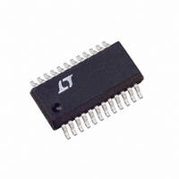
IC DC/DC CONTROLLER SYNC 24-SSOP
Manufacturer
Linear Technology
Type
Step-Down (Buck)r
Datasheet
1.LTC3713EGPBF.pdf
(24 pages)
Specifications of LTC3713EG
Internal Switch(s)
No
Synchronous Rectifier
Yes
Number Of Outputs
1
Voltage - Output
0.8 ~ 32.4 V
Current - Output
2A
Voltage - Input
1.5 ~ 36 V
Operating Temperature
-40°C ~ 85°C
Mounting Type
Surface Mount
Package / Case
24-SSOP
Lead Free Status / RoHS Status
Contains lead / RoHS non-compliant
Power - Output
-
Frequency - Switching
-
Available stocks
Company
Part Number
Manufacturer
Quantity
Price
Company:
Part Number:
LTC3713EG
Manufacturer:
LINEAR
Quantity:
208
Part Number:
LTC3713EG
Manufacturer:
LINEAR/凌特
Quantity:
20 000
Part Number:
LTC3713EG#PBF
Manufacturer:
LINEAR/凌特
Quantity:
20 000
Part Number:
LTC3713EG#TRPBF
Manufacturer:
LINEAR/凌特
Quantity:
20 000
APPLICATIO S I FOR ATIO
loss. For example, if R
loss will range from 1% up to 10% as the output current
varies from 1A to 10A for a 1.5V output.
2. Transition loss. This loss arises from the brief amount
of time the top MOSFET spends in the saturated region
during switch node transitions. It depends upon the input
voltage, load current, driver strength and MOSFET capaci-
tance, among other factors. The loss is significant at input
voltages above 20V and can be estimated from:
3. INTV
and control currents.
4. C
filtering the large RMS input current to the regulator. It
must have a very low ESR to minimize the AC I
sufficient capacitance to prevent the RMS current from
causing additional upstream losses in fuses or batteries.
Other losses, including C
conduction loss during dead time and inductor core loss
generally account for less than 2% additional loss.
When making adjustments to improve efficiency, the input
current is the best indicator of changes in efficiency. If you
make a change and the input current decreases, then the
efficiency has increased. If there is no change in input
current, then there is no change in efficiency.
Checking Transient Response
The regulator loop response can be checked by looking
at the load transient response. Switching regulators take
several cycles to respond to a step in load current. When
a load step occurs, V
equal to I
resistance of C
discharge C
by the regulator to return V
During this recovery time, V
overshoot or ringing that would indicate a stability
problem. The I
Figure 1 will provide adequate compensation for most
applications. For a detailed explanation of switching
control loop theory see Application Note 76.
Transition Loss (1.7A
IN
loss. The input capacitor has the difficult job of
CC
current. This is the sum of the MOSFET driver
LOAD
OUT
TH
OUT
(ESR), where ESR is the effective series
generating a feedback error signal used
U
pin external components shown in
. I
OUT
DS(ON)
LOAD
immediately shifts by an amount
OUT
U
–1
OUT
= 0.01 and R
) V
ESR loss, Schottky diode D1
also begins to charge or
OUT
IN
to its steady-state value.
2
can be monitored for
W
I
OUT
C
RSS
L
= 0.005 , the
2
f
U
R loss and
Design Example
As a design example, take a supply with the following
specifications: V
I
resistor with V
Next, use a standard value of 237k and choose the inductor
for about 40% ripple current at the maximum V
Selecting a standard value of 1 H results in a maximum
ripple current of:
Next, choose the synchronous MOSFET switch. Choosing
an IRF7811A (R
50 C/W) yields a nominal sense voltage of:
Tying V
for a nominal value of 100mV with current limit occurring
at 133mV. To check if the current limit is acceptable,
assume a junction temperature of about 10 C above a
50 C ambient with
and double check the assumed T
Now check the power dissipation of the top MOSFET at
current limit with
OUT(MAX)
V
T
R
I
P
L
LIMIT
BOT
J
SNS(NOM)
ON
I
L
= 50 C + (0.24W)(50 C/W) = 62 C
(
RNG
300
(
( . )(
300
= 6A, f = 300kHz. First, calculate the timing
0 24
2 5
3 3
kHz
to 1V will set the current sense voltage range
( . )( .
.
1 15 0 013
.
1 25
= (6A)(1.3)(0.013 ) = 101.4mV
1 25
V
kHz
V
( .
.
ON
2 5
.
3 3
133
W
)( . )( )
IN
– .
.
DS(ON)
300
0 4 6
= V
V
)(
1 25
V
V
= 1.8V to 3.3V, V
V
80 C
1
mV
– .
60 C
kHz
OUT
H
0 7
V
A
)
= 1.3:
= 0.013 , C
:
)(
= 1.15:
V
1
10 2
10
)
1
–
)
–
2
.
pF
1 25
3 3
2
1
1 25
.
A
3 3
.
)
( . )
.
2 6
.
J
V
2
V
in the MOSFET:
V
OUT
( . )( .
240
V
A
1 15 0 013
RSS
= 1.25V 100mV,
k
2 6
10 2
LTC3713
1 08
.
= 60pF,
.
A
.
A
H
IN
17
:
)
JA
3713fa
=


