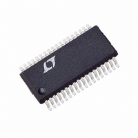
LTC1709EG#TR Linear Technology, LTC1709EG#TR Datasheet - Page 10

LTC1709EG#TR
Manufacturer Part Number
LTC1709EG#TR
Description
IC REG SW 2PH SYNC STPDWN 36SSOP
Manufacturer
Linear Technology
Type
Step-Down (Buck)r
Datasheet
1.LTC1709EG.pdf
(28 pages)
Specifications of LTC1709EG#TR
Internal Switch(s)
No
Synchronous Rectifier
Yes
Number Of Outputs
2
Voltage - Output
1.3 ~ 3.5 V
Current - Output
3A
Voltage - Input
4 ~ 36 V
Operating Temperature
-40°C ~ 85°C
Mounting Type
Surface Mount
Package / Case
36-SSOP
Lead Free Status / RoHS Status
Contains lead / RoHS non-compliant
Power - Output
-
Frequency - Switching
-
Available stocks
Company
Part Number
Manufacturer
Quantity
Price
LTC1709
OPERATIO
Main Control Loop
The LTC1709 uses a constant frequency, current mode
step-down architecture with inherent current sharing.
During normal operation, the top MOSFET is turned on
each cycle when the oscillator sets the RS latch, and
turned off when the main current comparator, I1, resets
the RS latch. The peak inductor current at which I1 resets
the RS latch is controlled by the voltage on the I
which is the output of the error amplifier EA. The differen-
tial amplifier, A1, produces a signal equal to the differential
voltage sensed across the output capacitor but re-refer-
ences it to the internal signal ground (SGND) reference.
The EAIN pin receives a portion of this voltage feedback
signal at the DIFFOUT as determined by VID logic input
pins (VID0 to VID4) and is compared to the internal
reference voltage by the EA. When the load current in-
creases, it causes a slight decrease in the EAIN pin voltage
relative to the 0.8V reference, which in turn causes the I
voltage to increase until the average inductor current
matches the new load current. After the top MOSFET has
turned off, the bottom MOSFET is turned on for the rest of
the period.
The top MOSFET drivers are biased from floating boot-
strap capacitor C
each off cycle through an external Schottky diode. When
V
may enter dropout and attempt to turn on the top MOSFET
continuously. A dropout detector detects this condition
and forces the top MOSFET to turn off for about 400ns
every 10th cycle to recharge the bootstrap capacitor, C
The main control loop is shut down by pulling Pin 1 (RUN/
SS) low. Releasing RUN/SS allows an internal 1.2 A
current source to charge soft-start capacitor C
C
I
value. As C
leased allowing normal operation to resume. When the
RUN/SS pin is low, all LTC1709 functions are shut down.
If V
has charged to 4.1V, an overcurrent latchoff can be
invoked as described in the Applications Information
section.
10
TH
IN
SS
OUT
voltage clamped at approximately 30% of its maximum
decreases to a voltage close to V
reaches 1.5V, the main control loop is enabled with the
has not reached 70% of its nominal value when C
SS
continues to charge, I
B
U
, which normally is recharged during
(Refer to Functional Diagram)
OUT
TH
, however, the loop
is gradually re-
SS
. When
TH
pin,
TH
SS
B
.
Low Current Operation
The LTC1709 operates in a continuous, PWM control
mode. The resulting operation at low output currents
optimizes transient response at the expense of substantial
negative inductor current during the latter part of the
period. The level of ripple current is determined by the
inductor value, input voltage, output voltage, and fre-
quency of operation.
Frequency Synchronization
The phase-locked loop allows the internal oscillator to be
synchronized to an external source via the PLLIN pin. The
output of the phase detector at the PLLFLTR pin is also the
DC frequency control input of the oscillator that operates
over a 140kHz to 310kHz range corresponding to a DC
voltage input from 0V to 2.4V. When locked, the PLL aligns
the turn on of the top MOSFET to the rising edge of the
synchronizing signal. When PLLIN is left open, the PLLFLTR
pin goes low, forcing the oscillator to minimum frequency.
Input capacitance ESR requirements and efficiency losses
are substantially reduced because the peak current drawn
from the input capacitor is effectively divided by two and
power loss is proportional to the RMS current squared. A
two stage, single output voltage implementation can re-
duce input path power loss by 75% and radically reduce
the required RMS current rating of the input capacitor(s).
INTV
Power for the top and bottom MOSFET drivers and most
of the IC circuitry is derived from INTV
EXTV
regulator supplies INTV
taken above 4.7V, the 5V regulator is turned off and an
internal switch is turned on connecting EXTV
This allows the INTV
efficiency external source such as the output of the regu-
lator itself or a secondary winding, as described in the
Applications Information section. An external Schottky
diode can be used to minimize the voltage drop from
EXTV
the specified INTV
applied to EXTV
CC
CC
CC
/EXTV
to INTV
pin is left open, an internal 5V low dropout
CC
CC
CC
Power
CC
for additional gate drive capability.
in applications requiring greater than
CC
current. Voltages up to 7V can be
power to be derived from a high
CC
power. If the EXTV
CC
CC
. When the
to INTV
CC
pin is
CC
.


