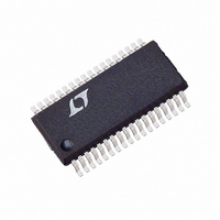
LTC1709EG#TR Linear Technology, LTC1709EG#TR Datasheet - Page 8

LTC1709EG#TR
Manufacturer Part Number
LTC1709EG#TR
Description
IC REG SW 2PH SYNC STPDWN 36SSOP
Manufacturer
Linear Technology
Type
Step-Down (Buck)r
Datasheet
1.LTC1709EG.pdf
(28 pages)
Specifications of LTC1709EG#TR
Internal Switch(s)
No
Synchronous Rectifier
Yes
Number Of Outputs
2
Voltage - Output
1.3 ~ 3.5 V
Current - Output
3A
Voltage - Input
4 ~ 36 V
Operating Temperature
-40°C ~ 85°C
Mounting Type
Surface Mount
Package / Case
36-SSOP
Lead Free Status / RoHS Status
Contains lead / RoHS non-compliant
Power - Output
-
Frequency - Switching
-
Available stocks
Company
Part Number
Manufacturer
Quantity
Price
LTC1709
PI FU CTIO S
AMPMD (Pin 23): This Logic Input pin controls the
connections of internal precision resistors that configure
the operational amplifier as a unity-gain differential
amplifier.
TG2, TG1 (Pins 24, 35): High Current Gate Drives for Top
N-Channel MOSFETS. These are the outputs of floating
drivers with a voltage swing equal to INTV
posed on the switch node voltage SW.
SW2, SW1 (Pins 25, 34): Switch Node Connections to
Inductors. Voltage swing at these pins is from a Schottky
diode (external) voltage drop below ground to V
BOOST 2, BOOST 1 (Pins 26, 33): Bootstrapped Supplies
to the Topside Floating Drivers. External capacitors are
connected between the Boost and Switch pins, and Schottky
diodes are connected between the Boost and INTV
BG2, BG1 (Pins 27, 31): High Current Gate Drives for
Bottom N-Channel MOSFETS. Voltage swing at these pins
is from ground to INTV
8
U
U
U
CC
.
CC
superim-
IN
CC
.
pins.
PGND (Pin 28): Driver Power Ground, connect to sources
of bottom N-channel MOSFETS and the (–) terminals of
C
INTV
Dropout Regulator and the EXTV
control circuits are powered from this voltage source.
Decouple to power ground with a 1 F ceramic capacitor
placed directly adjacent to the IC and minimum of 4.7 F
additional tantalum or other low ESR capacitor.
EXTV
Switch . This switch closes and supplies INTV
ing the internal low dropout regulator whenever EXTV
higher than 4.7V. See EXTV
tions Information section. Do not exceed 7V on this pin
and ensure V
V
to the IC’s signal ground pin.
IN
IN
.
(Pin 32): Main Supply Pin. Should be closely decoupled
CC
CC
(Pin 29): Output of the Internal 5V Linear Low
(Pin 30): External Power Input to an Internal
EXTVCC
V
IN
.
CC
Connection in the Applica-
CC
Switch. The driver and
CC,
bypass-
CC
is


