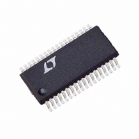
LTC1709EG#TR Linear Technology, LTC1709EG#TR Datasheet - Page 16

LTC1709EG#TR
Manufacturer Part Number
LTC1709EG#TR
Description
IC REG SW 2PH SYNC STPDWN 36SSOP
Manufacturer
Linear Technology
Type
Step-Down (Buck)r
Datasheet
1.LTC1709EG.pdf
(28 pages)
Specifications of LTC1709EG#TR
Internal Switch(s)
No
Synchronous Rectifier
Yes
Number Of Outputs
2
Voltage - Output
1.3 ~ 3.5 V
Current - Output
3A
Voltage - Input
4 ~ 36 V
Operating Temperature
-40°C ~ 85°C
Mounting Type
Surface Mount
Package / Case
36-SSOP
Lead Free Status / RoHS Status
Contains lead / RoHS non-compliant
Power - Output
-
Frequency - Switching
-
Available stocks
Company
Part Number
Manufacturer
Quantity
Price
APPLICATIO S I FOR ATIO
LTC1709
external voltage source is applied to the EXTV
the V
series with the LTC1709’s V
between the EXTV
from backfeeding V
Significant efficiency gains can be realized by powering
INTV
from the driver and control currents will be scaled by the
ratio: (Duty Factor)/(Efficiency). For 5V regulators this
means connecting the EXTV
ever, for 3.3V and other lower voltage regulators, addi-
tional circuitry is required to derive INTV
output.
The following list summarizes the four possible connec-
tions for EXTV
1. EXTV
to be powered from the internal 5V regulator resulting in
a significant efficiency penalty at high input voltages.
2. EXTV
connection for a 5V regulator and provides the highest
efficiency.
3. EXTV
supply is available in the 5V to 7V range, it may be used to
power EXTV
gate drive requirements.
4. EXTV
For 3.3V and other low voltage regulators, efficiency gains
can still be realized by connecting EXTV
derived voltage which has been boosted to greater than
16
Figure 5a. Secondary Output Loop with EXTV
CC
IN
OPTIONAL EXTV
5V < V
EXTV
CC
CC
CC
CC
supply is not present, a diode can be placed in
from the output, since the V
CC
SEC
left open (or grounded). This will cause INTV
connected to an output-derived boost network.
connected directly to V
connected to an external supply. If an external
LTC1709
CC
< 7V
CC:
providing it is compatible with the MOSFET
CC
PGND
CONNECTION
SW1
CC
BG1
TG1
U
V
IN
IN
and the V
.
C
IN
N-CH
N-CH
+
U
CC
IN
pin directly to V
pin and a Schottky diode
IN
V
1N4148
pin, to prevent current
OUT
IN
T1
W
IN
. This is the normal
CC
current resulting
CC
power from the
CC
R
SENSE
to an output-
V
Connection
CC
SEC
+
+
OUT
U
pin when
1709 F05a
. How-
1 F
C
V
OUT
OUT
CC
4.7V but less than 7V. This can be done with either the
inductive boost winding as shown in Figure 5a or the
capacitive charge pump shown in Figure 5b. The charge
pump has the advantage of simple magnetics.
Topside MOSFET Driver Supply (C
Functional Diagram)
External bootstrap capacitors C
the BOOST 1 and BOOST 2 pins supply the gate drive
voltages for the topside MOSFETs. Capacitor C
Functional Diagram is charged though diode D
INTV
turns on, the driver places the C
source of the desired MOSFET. This enhances the MOSFET
and turns on the topside switch. The switch node voltage,
SW, rises to V
The value of the boost capacitor C
times that of the total input capacitance of the topside
MOSFET(s). The reverse breakdown of D
than V
The final arbiter when defining the best gate drive ampli-
tude level will be the input supply current. If a change is
made that decreases input current, the efficiency has
improved. If the input current does not change then the
efficiency has not changed either.
Output Voltage
The LTC1709 has a true remote voltage sense capablity.
The sensing connections should be returned from the load
back to the differential amplifier’s inputs through a com-
CC
EXTV
IN(MAX).
when the SW pin is low. When the topside MOSFET
Figure 5b. Capacitive Charge Pump for EXTV
CC
LTC1709
IN
and the BOOST pin rises to V
PGND
SW1
BG1
TG1
V
IN
C
IN
N-CH
N-CH
+
B
B1
BAT85
V
voltage across the gate-
B
IN
and C
L1
needs to be 30 to 100
B
,D
VN2222LL
B
B
0.22 F
) (Refer to
B2
must be greater
R
SENSE
connected to
IN
+
+
+ V
CC
B
1709 F05b
BAT85
BAT85
B
INTVCC
C
V
OUT
in the
OUT
from
.


