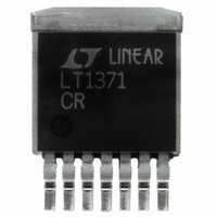
LT1371CR Linear Technology, LT1371CR Datasheet - Page 10

LT1371CR
Manufacturer Part Number
LT1371CR
Description
IC SWTCHNG REG 3A HI-EFF 7-DD
Manufacturer
Linear Technology
Type
Step-Down (Buck), Step-Up (Boost), Inverting, Cuk, Flyback, Forward Converterr
Datasheet
1.LT1371CRPBF.pdf
(16 pages)
Specifications of LT1371CR
Internal Switch(s)
Yes
Synchronous Rectifier
No
Number Of Outputs
1
Voltage - Output
1.25 ~ 35 V
Current - Output
3A
Frequency - Switching
500kHz
Voltage - Input
2.7 ~ 25 V
Operating Temperature
0°C ~ 70°C
Mounting Type
Surface Mount
Package / Case
D²Pak, TO-263 (7 leads + tab)
Lead Free Status / RoHS Status
Contains lead / RoHS non-compliant
Power - Output
-
Available stocks
Company
Part Number
Manufacturer
Quantity
Price
Company:
Part Number:
LT1371CR
Manufacturer:
LT
Quantity:
5 510
Part Number:
LT1371CR
Manufacturer:
LINEAR/凌特
Quantity:
20 000
Company:
Part Number:
LT1371CR#TRPBF
Manufacturer:
PHI
Quantity:
648
Part Number:
LT1371CR#TRPBF
Manufacturer:
LT/凌特
Quantity:
20 000
APPLICATIO S I FOR ATIO
LT1371
Output Capacitor Ripple Current (RMS)
Input Capacitors
The input capacitor of a boost converter is less critical due
to the fact that the input current waveform is triangular and
does not contain large squarewave currents as is found in
the output capacitor. Capacitors in the range of 10 F to
100 F, with an ESR of 0.2 or less, work well up to full 3A
switch current. Higher ESR capacitors may be acceptable
at low switch currents. Input capacitor ripple current for a
boost converter is :
The input capacitor can see a very high surge current when
a battery or high capacitance source is connected “live”
and solid tantalum capacitors can fail under this condition.
Several manufacturers have developed tantalum capaci-
tors specially tested for surge capability (AVX TPS series,
for instance) but even these units may fail if the input
voltage approaches the maximum voltage rating of the
capacitor during a high surge. AVX recommends derating
capacitor voltage by 2:1 for high surge applications.
Ceramic, OS-CON and aluminum electrolytic capacitors
may also be used and have a high tolerance to turn-on
surges.
Ceramic Capacitors
Higher value, lower cost ceramic capacitors are now
becoming available in smaller case sizes. These are tempt-
ing for switching regulator use because of their very low
ESR. Unfortunately, the ESR is so low that it can cause
loop stability problems. Solid tantalum capacitor ESR
10
DC = Switch Duty Cycle
I
I
f = 500kHz Switching Frequency
RIPPLE
RIPPLE
(RMS) = I
=
0.3(V
(f)(L)(V
= I
IN
U U
)(V
OUT
OUT
OUT
OUT
1 – DC
– V
V
)
DC
OUT
IN
V
)
IN
– V
W
IN
U
generates a loop “zero” at 5kHz to 50kHz that is instrumen-
tal in giving acceptable loop phase margin. Ceramic ca-
pacitors remain capacitive to beyond 300kHz and usually
resonate with their ESL before ESR becomes effective.
They are appropriate for input bypassing because of their
high ripple current ratings and tolerance of turn-on surges.
Output Diode
The suggested output diode (D1) is a 1N5821 Schottky or
its Motorola equivalent MBR330. It is rated at 3A average
forward current and 30V reverse voltage. Typical forward
voltage is 0.6V at 3A. The diode conducts current only
during switch OFF time. Peak reverse voltage for boost
converters is equal to regulator output voltage. Average
forward current in normal operation is equal to output
current.
Frequency Compensation
Loop frequency compensation is performed on the output
of the error amplifier (V
The main pole is formed by the series capacitor and the
output impedance ( 500k ) of the error amplifier. The
pole falls in the range of 2Hz to 20Hz. The series resistor
creates a “zero” at 1kHz to 5kHz, which improves loop
stability and transient response. A second capacitor, typi-
cally one-tenth the size of the main compensation capaci-
tor, is sometimes used to reduce the switching frequency
ripple on the V
voltage ripple attenuated by the output divider and multi-
plied by the error amplifier. Without the second capacitor,
V
To prevent irregular switching, V
kept below 50mV
C
V
V
g
R
V
pin ripple is:
m
C
RIPPLE
OUT
C
Pin Ripple =
= Series resistor on V
= Error amplifier transconductance
( 1500 mho)
= DC output voltage
= Output ripple (V
C
P–P
pin. V
1.245(V
. Worst-case V
C
C
pin ripple is caused by output
pin) with a series RC network.
RIPPLE
(V
C
P–P
OUT
pin
C
)
)(g
)
C
pin ripple should be
pin ripple occurs at
m
)(R
C
)


