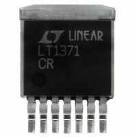
LT1371CR Linear Technology, LT1371CR Datasheet - Page 8

LT1371CR
Manufacturer Part Number
LT1371CR
Description
IC SWTCHNG REG 3A HI-EFF 7-DD
Manufacturer
Linear Technology
Type
Step-Down (Buck), Step-Up (Boost), Inverting, Cuk, Flyback, Forward Converterr
Datasheet
1.LT1371CRPBF.pdf
(16 pages)
Specifications of LT1371CR
Internal Switch(s)
Yes
Synchronous Rectifier
No
Number Of Outputs
1
Voltage - Output
1.25 ~ 35 V
Current - Output
3A
Frequency - Switching
500kHz
Voltage - Input
2.7 ~ 25 V
Operating Temperature
0°C ~ 70°C
Mounting Type
Surface Mount
Package / Case
D²Pak, TO-263 (7 leads + tab)
Lead Free Status / RoHS Status
Contains lead / RoHS non-compliant
Power - Output
-
Available stocks
Company
Part Number
Manufacturer
Quantity
Price
Company:
Part Number:
LT1371CR
Manufacturer:
LT
Quantity:
5 510
Part Number:
LT1371CR
Manufacturer:
LINEAR/凌特
Quantity:
20 000
Company:
Part Number:
LT1371CR#TRPBF
Manufacturer:
PHI
Quantity:
648
Part Number:
LT1371CR#TRPBF
Manufacturer:
LT/凌特
Quantity:
20 000
APPLICATIO S I FOR ATIO
LT1371
Shutdown and Synchronization
The 7-pin R and T7 package devices have a dual function
S/S pin which is used for both shutdown and synchroni-
zation. The SW package device has both a Shutdown
(SHDN) pin and a Synchronization (SYNC) pin which can
be used separately or tied together. These pins are logic
level compatible and can be pulled high, tied to V
floating for normal operation. A logic low on the S/S pin or
SHDN pin activates shutdown, reducing the part’s supply
current to 12 A. Typical synchronization range is from
1.05 to 1.8 times the part’s natural switching frequency,
but is only guaranteed between 600kHz and 800kHz. A
12 s resetable shutdown delay network guarantees the
part will not go into shutdown while receiving a synchro-
nization signal when the functions are combined.
Caution should be used when synchronizing above 700kHz
because at higher sync frequencies the amplitude of the
internal slope compensation used to prevent subharmonic
switching is reduced. This type of subharmonic switching
only occurs when the duty cycle of the switch is above 50%.
Higher inductor values will tend to eliminate problems.
Thermal Considerations
Care should be taken to ensure that the worst-case input
voltage and load current conditions do not cause exces-
sive die temperatures. Typical thermal resistance is
30 C/W for the R package and 50 C/W for the SW and T7
packages but these numbers will vary depending on the
mounting techniques (copper area, air flow, etc.). Heat is
transferred from the R and T7 packages via the tab and
from the SW package via pins 4 to 7 and 14 to 17.
Average supply current (including driver current) is:
Switch power dissipation is given by:
8
I
I
DC = switch duty cycle
P
R
IN
SW
SW
SW
= 4mA + DC [I
= switch current
= (I
= output switch ON resistance
SW
)
2
(R
SW
U U
SW
)(DC)
/60 + I
SW
(0.004)]
W
U
IN
or left
Total power dissipation of the die is the sum of supply
current times supply voltage, plus switch power:
Surface mount heat sinks are also becoming available
which can lower package thermal resistance by 2 or 3
times. One manufacturer is Wakefield Engineering who
offers surface mount heat sinks for both the R package
(DD) and SW package (SW20) and can be reached at (617)
245-5900.
Choosing the Inductor
For most applications the inductor will fall in the range of
2.2 H to 22 H. Lower values are chosen to reduce physi-
cal size of the inductor. Higher values allow more output
current because they reduce peak current seen by the
power switch, which has a 3A limit. Higher values also
reduce input ripple voltage and reduce core loss.
When choosing an inductor you might have to consider
maximum load current, core and copper losses, allowable
component height, output voltage ripple, EMI, fault
current in the inductor, saturation and, of course, cost.
The following procedure is suggested as a way of handling
these somewhat complicated and conflicting requirements.
1. Assume that the average inductor current for a boost
2. Calculate peak inductor current at full load current to
P
converter is equal to load current times V
decide whether or not the inductor must withstand
continuous overload conditions. If average inductor
current at maximum load current is 1A, for instance, a
1A inductor may not survive a continuous 3A overload
condition. Also be aware that boost converters are not
short-circuit protected and that, under output short
conditions, inductor current is limited only by the
available current of the input supply.
ensure that the inductor will not saturate. Peak current
can be significantly higher than output current, espe-
cially with smaller inductors and lighter loads, so don’t
omit this step. Powdered iron cores are forgiving
because they saturate softly, whereas ferrite cores
D(TOTAL)
= (I
IN
)(V
IN
) + P
SW
OUT
/ V
IN
and


