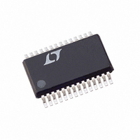
LTC1142HVCG-ADJ Linear Technology, LTC1142HVCG-ADJ Datasheet - Page 12

LTC1142HVCG-ADJ
Manufacturer Part Number
LTC1142HVCG-ADJ
Description
IC SW REG STEP-DOWN DUAL 28-SSOP
Manufacturer
Linear Technology
Type
Step-Down (Buck)r
Datasheet
1.LTC1142CG.pdf
(20 pages)
Specifications of LTC1142HVCG-ADJ
Internal Switch(s)
No
Synchronous Rectifier
Yes
Number Of Outputs
2
Voltage - Output
3.3V, 5V
Current - Output
50mA
Frequency - Switching
250kHz
Voltage - Input
3.5 ~ 18 V
Operating Temperature
0°C ~ 70°C
Mounting Type
Surface Mount
Package / Case
28-SSOP
Lead Free Status / RoHS Status
Contains lead / RoHS non-compliant
Power - Output
-
Available stocks
Company
Part Number
Manufacturer
Quantity
Price
Part Number:
LTC1142HVCG-ADJ
Manufacturer:
LT/凌特
Quantity:
20 000
APPLICATIO S I FOR ATIO
LTC1142/LTC1142L/LTC1142HV
dead-time, which could cost as much as 1% in efficiency
(although there are no other harmful effects if D1 and D2
are omitted). Therefore, D1 and D2 should be selected for
a forward voltage of less than 0.6V when conducting I
C
In continuous mode, the source current of the P-channel
MOSFET is a square wave of duty cycle V
prevent large voltage transients, a low ESR input capaci-
tor sized for the maximum RMS current must be used. The
maximum RMS capacitor current is given by:
This formula has a maximum at V
I
monly used for design because even significant deviations
do not offer much relief. Note that capacitor manufacturer’s
ripple current ratings are often based on only 2000 hours
of life. This makes it advisable to further derate the
capacitor, or to choose a capacitor rated at a higher
temperature than required. Several capacitors may also be
paralleled to meet size or height requirements in the
design. Always consult the manufacturer if there is any
question. An additional 0.1 F to 1 F ceramic capacitor is
also required on each V
frequency decoupling.
The selection of C
Series Resistance (ESR). The ESR of C
than twice the value of R
LTC1142:
Optimum efficiency is obtained by making the ESR equal
to R
efficiency degrades by less than 1%. If the ESR is greater
than 2R
will prematurely trigger Burst Mode operation, resulting in
disruption of continuous mode and an efficiency hit which
can be several percent.
Manufacturers such as Nichicon and United Chemicon
should be considered for high performance capacitors.
The OS-CON semiconductor dielectric capacitor available
12
RMS
IN
C
C
and C
OUT
IN
SENSE
= I
Required I
SENSE
OUT
Required ESR < 2R
OUT
. As the ESR is increased up to 2R
/2. This simple worst case conditon is com-
, the voltage ripple on the output capacitor
Selection
RMS
OUT
U
is driven by the required Effective
IN
SENSE
I
MAX
U
line (Pins 10 and 24) for high
SENSE
for proper operation of the
V
OUT
W
V
IN
IN
OUT
V
= 2V
IN
V
must be less
OUT
OUT
OUT
SENSE
U
/ V
, where
1 2 /
IN
, the
MAX
. To
.
from Sanyo has the lowest ESR/size ratio of any aluminum
electrolytic at a somewhat higher price. Once the ESR
requirement for C
rating generally far exceeds the I
In surface mount applications multiple capacitors may
have to be parallel to meet the capacitance, ESR or RMS
current handling requirements of the application. Alumi-
num electrolytic and dry tantalum capacitors are both
available in surface mount configurations. In the case of
tantalum, it is critical that the capacitors are surge tested
for use in switching power supplies. An excellent choice
is the AVX TPS series of surface mount tantalums, avail-
able in case heights ranging from 2mm to 4mm. For
example, if 200 F/10V is called for in an application
requiring 3mm height, two AVX 100 F/10V (P/N TPSD
107K010) could be used. Consult the manufacturer for
other specific recommendations.
At low supply voltages, a minimum capacitance at C
needed to prevent an abnormal low frequency operating
mode (see Figure 4). When C
output ripple at low frequencies will be large enough to trip
the voltage comparator. This causes Burst Mode opera-
tion to be activated when the LTC1142 would normally be
in continuous operation. The output remains in regulation
at all times.
Checking Transient Response
The regulator loop response can be checked by looking
at the load transient response. Switching regulators take
several cycles to respond to a step in DC (resistive) load
1000
800
600
400
200
Figure 4. Minimum Value of C
0
0
OUT
1
L = 25 H
R
R
V
has been met, the RMS current
SENSE
SENSE
IN
– V
L = 50 H
2
OUT
= 0.02
= 0.05
L = 50 H
R
SENSE
OUT
VOLTAGE (V)
RIPPLE(P-P)
3
= 0.02
is made too small, the
4
OUT
1142 F04
requirement.
5
OUT
is


