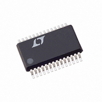
LTC1142HVCG-ADJ Linear Technology, LTC1142HVCG-ADJ Datasheet - Page 9

LTC1142HVCG-ADJ
Manufacturer Part Number
LTC1142HVCG-ADJ
Description
IC SW REG STEP-DOWN DUAL 28-SSOP
Manufacturer
Linear Technology
Type
Step-Down (Buck)r
Datasheet
1.LTC1142CG.pdf
(20 pages)
Specifications of LTC1142HVCG-ADJ
Internal Switch(s)
No
Synchronous Rectifier
Yes
Number Of Outputs
2
Voltage - Output
3.3V, 5V
Current - Output
50mA
Frequency - Switching
250kHz
Voltage - Input
3.5 ~ 18 V
Operating Temperature
0°C ~ 70°C
Mounting Type
Surface Mount
Package / Case
28-SSOP
Lead Free Status / RoHS Status
Contains lead / RoHS non-compliant
Power - Output
-
Available stocks
Company
Part Number
Manufacturer
Quantity
Price
Part Number:
LTC1142HVCG-ADJ
Manufacturer:
LT/凌特
Quantity:
20 000
OPERATIO
As the load current increases, the output voltage de-
creases slightly. This causes the output of the gain stage
[Pin 27(13)] to increase the current comparator thresh-
old, thus tracking the load current.
The sequence of events for Burst Mode operation is very
similar to continuous operation with the cycle interrupted
by the voltage comparator. When the output voltage is at
or above the desired regulated value, the P-channel
MOSFET is held off by comparator V and the timing
capacitor continues to discharge below V
timing capacitor discharges past V
tor S trips, causing the internal sleep line to go low and the
N-channel MOSFET to turn off.
The circuit now enters sleep mode with both power
MOSFETs turned off. In sleep mode a majority of the
circuitry is turned off, dropping the quiescent current
from 1.6mA to 160 A (for one regulator block). The load
current is now being supplied from the output capacitor.
When the output voltage has dropped by the amount of
APPLICATIO S I FOR ATIO
The basic LTC1142 application circuit is shown in
Figure 1. External component selection is driven by the
load requirement and begins with the selection of R
Once R
power MOSFETs and D1 are selected. Finally, C
C
3.3V and 5V sections in the LTC1142 are identical and
similarly section 1 and section 2 in the LTC1142HV-ADJ/
LTC1142L-ADJ are identical, the process of component
selection is the same for both sections. The circuit shown
in Figure 1 can be configured for operation up to an input
voltage of 20V.
R
R
The LTC1142 current comparators have a threshold range
which extends from a minimum of 25mV/R
maximum of 150mV/R
threshold sets the peak of the inductor ripple current,
OUT
SENSE
SENSE
are selected and the loop is compensated. Since the
SENSE
Selection for Output Current
is chosen based on the required output current.
is known, C
U
U
Refer to Functional Diagram
SENSE
T
U
and L can be chosen. Next, the
. The current comparator
TH2
W
, voltage compara-
TH1
. When the
SENSE
U
IN
SENSE
to a
and
.
hysteresis in comparator V, the P-channel MOSFET is
again turned on and this process repeats.
To avoid the operation of the current loop interfering with
Burst Mode operation, a built-in offset V
in the gain stage. This prevents the current comparator
threshold from increasing until the output voltage has
dropped below a minimum threshold.
To prevent both the external MOSFETs from ever being
turned on at the same time, feedback is incorporated to
sense the state of the driver output pins. Before the NDrive
output can go high, the PDrive output must also be high.
Likewise, the PDrive output is prevented from going low
while the NDrive output is high.
Using constant off-time architecture, the operating fre-
quency is a function of the input voltage. To minimize the
frequency variation as dropout is approached, the off-time
controller increases the discharge current as V
below V
turned on continuously (100% duty cycle) providing low
dropout operation with V
yielding a maximum output current I
value less half the peak-to-peak ripple current. For proper
Burst Mode operation, I
equal to the minimum current comparator threshold.
Since efficiency generally increases with ripple current,
the maximum allowable ripple current is assumed, i.e.,
I
Operating Frequency section). Solving for R
allowing a margin for variations in the LTC1142 and
external component values yields:
A graph for Selecting R
is given in Figure 2.
The load current below which Burst Mode operation com-
mences, I
RIPPLE(P-P)
LTC1142/LTC1142L/LTC1142HV
R
SENSE
OUT
BURST
=
= 25mV/R
+ 1.5V. In dropout the P-channel MOSFET is
100mV
I
MAX
, and the peak short-circuit current I
SENSE
SENSE
RIPPLE(P-P)
OUT
vs Maximum Output Current
(see C
~ V
IN
.
T
must be less than or
MAX
and L Selection for
OS
equal to the peak
is incorporated
SENSE
IN
SC(PK)
drops
9
and
,


