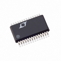
LTC1142HVCG-ADJ Linear Technology, LTC1142HVCG-ADJ Datasheet - Page 17

LTC1142HVCG-ADJ
Manufacturer Part Number
LTC1142HVCG-ADJ
Description
IC SW REG STEP-DOWN DUAL 28-SSOP
Manufacturer
Linear Technology
Type
Step-Down (Buck)r
Datasheet
1.LTC1142CG.pdf
(20 pages)
Specifications of LTC1142HVCG-ADJ
Internal Switch(s)
No
Synchronous Rectifier
Yes
Number Of Outputs
2
Voltage - Output
3.3V, 5V
Current - Output
50mA
Frequency - Switching
250kHz
Voltage - Input
3.5 ~ 18 V
Operating Temperature
0°C ~ 70°C
Mounting Type
Surface Mount
Package / Case
28-SSOP
Lead Free Status / RoHS Status
Contains lead / RoHS non-compliant
Power - Output
-
Available stocks
Company
Part Number
Manufacturer
Quantity
Price
Part Number:
LTC1142HVCG-ADJ
Manufacturer:
LT/凌特
Quantity:
20 000
APPLICATIO S I FOR ATIO
may be loaded without regard to the primary output load,
providing that the loop remains in continuous mode
operation.
Burst Mode operation can be suppressed at low output
currents with a simple external network which cancels the
25mV minimum current comparator threshold. This tech-
nique is also useful for eliminating audible noise from
certain types of inductors in high current (I
applications when they are lightly loaded.
An external offset is put in series with the Sense
subtract from the built-in 25mV offset. An example of this
technique is shown in Figure 10. Two 100 resistors are
inserted in series with the sense leads from the sense
resistor.
TYPICAL APPLICATIO S
3.6V/2A
V
220 F
C
OUT1
OUT1
10V
2
Figure 10. Suppression of Burst Mode Operation
[PIN 28(14)]
+
52.3k
[PIN 1(15)]
R
100k
0.05
SENSE1
1%
1%
R2
R1
SENSE
SENSE
+
–
+
MBRS130T3
27 H
100pF
C
22 F
35V
L1
U
IN1
2
R
L1: SUMIDA CDRH125-270
L2: SUMIDA CDRH125-330
R3
SENSE1,
1000pF
D1
R
U
Figure 11. LTC1142HV-ADJ Dual Regulator with 3.6V/2A and 5V/2A Outputs
SENSE2
100
100
N-CH
Si9410DY
1000pF
P-CH
Si9430DY
R2
R1
: DALE WSL-2010-.05
0.22 F
U
W
23
28
1
2
6
SENSE
PDRIVE 1
SENSE
NDRIVE 1
PGND1 SGND1 C
V
V
FB1
+
(For additional high efficiency circuits, see Application Note 54)
IN1
5
24
R
+
–
1142 F10
1
SENSE
C
1
OUT
V
OUT
OUT
4
U
SHDN1
–
> 5A)
T1
pin to
25
C
270pF
3
T1
0V = NORMAL
>1.5V = SHDN
LTC1142HV-ADJ
5.2V TO 18V
I
TH1
27
C
3300pF
R
1k
C1
V
C1
IN
I
TH2
With the addition of R3 a current is generated through R1
causing an offset of:
If V
Burst Mode operation is prevented from occurring. Since
V
decreased by the same offset. Thus, to get back to the
same I
To prevent noise spikes from erroneously tripping the
current comparator, a 1000pF capacitor is needed across
Pins 1 (15) and Pins 28 (14).
13
C
3300pF
LTC1142/LTC1142L/LTC1142HV
R
1k
OFFSET
C2
C2
R
SHDN2
V
OFFSET
C
OFFSET
SENSE
T2
11
17
C
270pF
T2
MAX
SGND2 PGND2
is constant, the maximum load current is also
> 25mV, the built-in offset will be cancelled and
, the value of the sense resistor must be lower:
18
PDRIVE 2
SENSE
NDRIVE 2
SENSE
75
I
V
V
MAX
IN2
V
OUT
19
10
FB2
mV
–
+
2
2
15
14
20
9
16
0.22 F
Si9410DY
Si9430DY
R
1000pF
1
N-CH
P-CH
R
1
R
3
D2
MBRS130T3
33 H
100pF
L2
+
C
22 F
35V
IN2
2
R
0.05
SENSE2
R4
150k
1%
R3
49.9k
1%
+
17
C
220 F
10V
1142 F11
V
5V/2A
OUT2
2
OUT2


