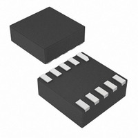
MAX4959ELB+T Maxim Integrated Products, MAX4959ELB+T Datasheet - Page 6

MAX4959ELB+T
Manufacturer Part Number
MAX4959ELB+T
Description
IC CTLR HI VOLTAGE OVP 10-UDFN
Manufacturer
Maxim Integrated Products
Type
Overvoltage Protection Controllerr
Datasheet
1.MAX4959ELBT.pdf
(17 pages)
Specifications of MAX4959ELB+T
Applications
PC's, PDA's
Mounting Type
Surface Mount
Package / Case
10-µDFN
Lead Free Status / RoHS Status
Lead free / RoHS Compliant
Other names
MAX4959ELB+T
MAX4959ELB+TTR
MAX4959ELB+TTR
no blanking time for OVP, but the debounce time
applies once the IN voltage falls below V
above V
V
In this case, when the adapter is plugged in, the device
goes through a 20ms (typ) debounce time and ensures
that the voltage at IN is between V
before P1 is turned on. In this state, the CB pin controls
both P1 and P2.
High-Voltage OVP with Battery Switchover
6
OVLO
_______________________________________________________________________________________
, the CB pin does not control P1.
UVLO
OVS
UVS
V
DD
. When the voltage at IN is higher than
Correct Adapter (V
MAX4959
IN
N
VREF2 = 0.7V
VREF1 = 2V
UVLO
UVLO
+
-
+
-
< V
+
-
IN
V
and V
SG
OVLO
< V
OVLO
POWER
UVLO
OVLO
V
ON
DD
but
BANDGAP
)
OFF STORAGE
POWER-ON
RESET AND
ANALOG
SUPPLY
If the adapter has the correct voltage but not enough
power (incorrect low-power adapter), the MAX4959/
MAX4960 protect pFET P1 from oscillation. When the
adapter is first plugged in, P1 is off so the voltage is cor-
rect. When P1 is turned on after the debounce time, the
low-power adapter is dragged down to below V
The device waits for a 10ms blanking time to make sure
it is not a temporary glitch, and, if a fault still exists, it
latches off P1. P1 does not turn on again until the
adapter is unplugged (V
again. This feature can work without the battery present
+
-
DIGITAL
SUPPLY
Functional Diagram for the MAX4959
+
-
GATE1
Low-Power Adapter or Glitch Condition
N1
UVLOINT
OVLO
+
-
Functional Diagrams
IN
UVLO
< ~0.75V) and plugged in
LOGIC
N2
GATE2
CB
GND
UVLO
.


