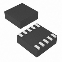
MAX4959ELB+T Maxim Integrated Products, MAX4959ELB+T Datasheet - Page 9

MAX4959ELB+T
Manufacturer Part Number
MAX4959ELB+T
Description
IC CTLR HI VOLTAGE OVP 10-UDFN
Manufacturer
Maxim Integrated Products
Type
Overvoltage Protection Controllerr
Datasheet
1.MAX4959ELBT.pdf
(17 pages)
Specifications of MAX4959ELB+T
Applications
PC's, PDA's
Mounting Type
Surface Mount
Package / Case
10-µDFN
Lead Free Status / RoHS Status
Lead free / RoHS Compliant
Other names
MAX4959ELB+T
MAX4959ELB+TTR
MAX4959ELB+TTR
The MAX4959/MAX4960 are used with a single MOS-
FET configuration as shown in the Typical Operating
Circuits to regulate voltage as a low-cost solution.
The MAX4959/MAX4960 are designed with pFETs. For
lower on-resistance, the external MOSFET can be multi-
ple pFETs in parallel. In most situations, MOSFETs with
R
MOSFETs (with V
range of the MAX4959/MAX4960.
The MAX4959/MAX4960 include undervoltage and
overvoltage comparators for window detection (see
Figure 4). GATE1 is enhanced and after the debounce
time, the pFET is turned on when the monitored voltage
is within the selected window.
The resistor values R1, R2, and R3 can be calculated
as follows:
where R
Use the following steps to determine the values for R1,
R2, and R3:
1) Choose a value for R
2) Calculate R3 based on R
3) Calculate R2 based on R
4) Calculate R1 based on R
DS(ON)
R3. Because the MAX4959/MAX4960 have very
high input impedance, R
V
V
OVLO
UVLO
MOSFET Configuration and Selection
TOTAL
specified for a V
trip point:
trip point:
Overvoltage/Undervoltage Window
V
V
High-Voltage OVP with Battery Switchover
UVLO
OVLO
R
R1 = R
R
= R1 + R2 + R3.
2
3
Applications Information
DS
_______________________________________________________________________________________
O
U
TOTAL
≥ 30V) withstand the full +28V IN
V
V
U
REF
O
REF
V
V
V
TOTAL
REF
REF
V
OVLO
UVLO
GS
– R2 – R3
Resistor Selection for
TOTAL
TOTAL
TOTAL
R
R
TOTAL
of 4.5V work well. Also,
R
R
, the sum of R1, R2, and
TOTAL
R
TOTAL
2
TOTAL
TOTAL
R
, R2, and R3:
, R3, and the desired
can be up to 5MΩ.
3
R
3
and the desired
R
3
Note that the ratio between the externally set OVLO and
UVLO threshold must not exceed:
V
minimum external adjustable UVLO trip threshold is
+5V, the V
V
The capacitor at V
power to the device for an external settable time,
t
have a minimum time of t
The worst case scenario is where V
- 0.8V = +4.2V, I
20ms, C = (10µA x 20ms) / (4.2V - 2.2V) = 100nF.
Note: The capacitor must be greater than 100nF for the
internal regulator to be stable, and needs to have low
ESR and low leakage current, for example, a ceramic
capacitor.
For most applications, bypass IN to GND with a 1µF
ceramic capacitor. If the power source has significant
inductance due to long lead length, take care to pre-
vent overshoots due to the LC tank circuit, and provide
protection if necessary to prevent exceeding the +30V
absolute maximum rating on V
The MAX4959/MAX4960 provide protection against volt-
age faults up to+28V, but this does not include negative
voltages. If negative voltages are a concern, connect a
Schottky diode from IN to GND to clamp negative input
voltages.
The MAX4959/MAX4960 are protected from ±15kV
Human Body Model ESD on IN when IN is bypassed to
ground with a 1µF ceramic capacitor.
Figure 2 shows the Human Body Model and Figure 3
shows the current waveform it generates when dis-
charged into a low impedance. This model consists of a
100pF capacitor charged to the ESD voltage of interest
that is then discharged into the device through a 1.5kΩ
resistor.
HOLD
DD
DD
V
V
is:
is regulated to +5V by a linear regulator. Since the
DD
DD
, when V
= V
= +5V
C = (I
DD
IN
– 0.8V
4 [V
range is +5V to +28V and the value at
VDD
IN
VDD
drops to 0V. The capacitor value to
DD
OVLO
x t
= 10µA (max). For a t
HOLD
must be large enough to provide
IN Bypass Considerations
V
/ V
HOLD
DD
) / (V
UVLO
ESD Test Conditions
Capacitor Selection
where V
where V
IN
Human Body Model
is:
DD
.
]
MAX
- V
IN
DD
≤ 4
= +5V, V
IN
IN
UVLO)
= 5V to 5.8V
> 5.8V
HOLD
DD
time of
= V
IN
9


