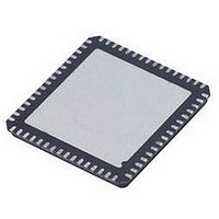
AD9267BCPZ Analog Devices Inc, AD9267BCPZ Datasheet - Page 17

AD9267BCPZ
Manufacturer Part Number
AD9267BCPZ
Description
IC MOD SIGMA-DELTA DUAL 64LFCSP
Manufacturer
Analog Devices Inc
Datasheet
1.AD9267BCPZRL7.pdf
(24 pages)
Specifications of AD9267BCPZ
Applications
*
Mounting Type
Surface Mount
Package / Case
64-LFCSP
Resolution (bits)
16bit
Sampling Rate
640MSPS
Input Channel Type
Differential
Data Interface
Serial, SPI
Supply Voltage Range - Analog
1.7V To 1.9V
Supply Voltage Range - Digital
1.7V To 1.9V
Lead Free Status / RoHS Status
Lead free / RoHS Compliant
Table 10. PLLMULTx Pins and PLL Multiplication Factor
PLLMULT[4:0] Pins
0
1
2
3
4
5
6
7
8
9
10
11
12
13
14
15
16
17 to 30
31
POWER DISSIPATION AND STANDBY MODE
The AD9267 consumes 415 mW. This power consumption can
be further reduced by configuring the chip in channel power-
down, standby, or sleep mode. The low power modes turn off
internal blocks of the chip including the reference. As a result,
the wake-up time is dependent on the amount of circuitry that
is turned off. Fewer internal circuits powered down result in
proportionally shorter wake-up time. The different low power
modes are shown in Table 11. In the standby mode, all clock
related activity is disabled in addition to each channel; the
references and LVDS outputs remain powered up to ensure a
short recovery and link integrity, respectively. During sleep
mode, all internal circuits are powered down, putting the device
into its lowest power mode; the LVDS outputs are disabled.
Each ADC channel can be independently powered down or
both channels can be set simultaneously by writing to the
channel index, Register 0x05[1:0]. Additionally, if the serial
port interface is not available, each channel can be indepen-
dently configured by tying the PDWNA (Pin 3) or PDWNB
(Pin 4) high.
Table 11. Low Power Modes
Mode
Normal
Channel Power-Down
Standby
Sleep
PLL Multiplication Factors (N)
8
9
10
12
14
15
16
17
18
20
21
24
25
28
30
32
34
42
Direct clocking
0x08[1:0]
0x0
0x1
0x2
0x3
Analog
Circuitry
On
Off
Off
Off
Clock
On
On
Off
Off
Ref.
On
On
On
Off
Rev. 0 | Page 17 of 24
DIGITAL OUTPUTS
Digital Output Format
The AD9267 digital bus outputs twos complement, single data
rate, LVDS data at 640 MSPS. The output is four bits wide per
channel.
The AD9267 supports both the ANSI-644 and a reduced power
data format similar to the IEEE1596.3 standard. The default
configuration at power-up is ANSI-644. This can be changed to
a low power reduced signal option by addressing Register
0x14[7], DRVSTD.
The LVDS driver current is derived on chip and sets the output
current at each output equal to a nominal 3.5 mA for the ANSI-
644 standard. A 100 Ω differential termination resistor placed at
the LVDS receiver inputs result in a nominal 350 mV swing at
the receiver. In the reduced power data format, the output swing
is limited to 200 mV and the resulting output current into the
100 Ω termination is 2 mA. As a result of the reduced LVDS
voltage swing, an additional 25% digital power savings can be
achieved over the ANSI-644 standard.
The desired output format can be selected by addressing
Register 0x14[7], DRVSTD. The LVDSTERM bits, Register
0x15[5:4], provide either 100 Ω or 200 Ω, or no termination
at the output of the data bus. Selecting the appropriate termina-
tion resistor is important to allow maximum signal transfer and
to minimize reflections for signal integrity. This can be achieved
by selecting a termination resistor that impedance matches the
termination of the receiver.
Overrange (OR) Condition
An overrange condition can be triggered by large in-band signals
that exceed the full-scale range of the Σ-Δ modulator, or it
can be triggered by out-of-band signals gained by the transfer
characteristics of the modulator. Figure 43 shows the signal
transfer function of the Σ-Δ modulator. The modulator output
possesses out-of-band gain above 10 MHz. As a result, the input
signal may exceed full scale for input frequencies beyond 10 MHz
and the ADC may be in an overrange state. The OR±x pins
serve as indicators for the overrange condition.
The OR±x pins are synchronous outputs that are updated at the
output data rate. The pins indicate whether an overrange condi-
tion has occurred within the AD9267. Ideally, OR±x should be
latched on the falling edge of DCO± to ensure proper setup-and-
hold time. However, because an overrange condition typically
extends well beyond one clock cycle (that is, does not toggle at
the DCO± rate); data can usually be successfully detected on
the rising edge of DCO± or monitored asynchronously. The
user has the ability to select how the overrange condition is
reported and this is controlled through the SPI bits (AUTORST,
OR_IND1, and OR_IND2) in Register 0x111[7:5]. The two
modes of operation are normal and data valid mode.
AD9267


