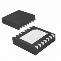
MAX4920BETD+T Maxim Integrated Products, MAX4920BETD+T Datasheet - Page 2

MAX4920BETD+T
Manufacturer Part Number
MAX4920BETD+T
Description
IC CTLR OVP/OCP BATT PWR 14-TDFN
Manufacturer
Maxim Integrated Products
Datasheet
1.MAX4921BETDT.pdf
(19 pages)
Specifications of MAX4920BETD+T
Applications
*
Mounting Type
Surface Mount
Package / Case
14-TDFN Exposed Pad
Lead Free Status / RoHS Status
Lead free / RoHS Compliant
ABSOLUTE MAXIMUM RATINGS
IN to GND ...............................................................-0.3V to +30V
GP1, GN1 to GND ..................................................-0.3V to +12V
IN to GP1 ................................................................-0.3V to +20V
BTO to GND ..........................................................-0.3V to +6.1V
BTI to BTO ................................................................-0.3V to +6V
BTI,
HP_PWR, ONOK, PWR_HOLD to GND ....................-0.3V to +6V
Battery Power-Up Logic with Overvoltage
and Overcurrent Protection
ELECTRICAL CHARACTERISTICS
(V
are at T
Stresses beyond those listed under “Absolute Maximum Ratings” may cause permanent damage to the device. These are stress ratings only, and functional
operation of the device at these or any other conditions beyond those indicated in the operational sections of the specifications is not implied. Exposure to
absolute maximum rating conditions for extended periods may affect device reliability.
2
Input Voltage Range
Input Supply Current
UVLO Supply Current
Shutdown Supply Current
IN Undervoltage Lockout
IN Undervoltage Lockout
Hysteresis
Overvoltage Trip Level
IN Overvoltage Lockout
Hysteresis
BATTERY SWITCHOVER
BTI Input Range
BTI UVLO
BTI UVLO Hysteresis
BTI Low-Battery Threshold
BTI Low-Battery Hysteresis
BTI Supply Current
BTI Shutdown Current
INTERNAL pFET
Switch On-Resistance
Forward-Overload Current Limit
IN
_______________________________________________________________________________________
ACOK, PWR_ON, EN to GND ...........................-0.3V to +6V
= 5V (MAX4919B/MAX4920B) or V
A
= +25°C.) (Note 1)
PARAMETER
SYMBOL
V
V
V
V
I
IN
SHDN
I
V
R
UVBTI
UVLO
OVLO
LVBTI
I
V
UVL
I
LIM
BTI
ON
IN
= 4.2V (MAX4921B), V
IN
MAX4919B/MAX4920B
MAX4921B
V
V
V
V
V
V
V
Adapter out, V
EN = high
V
V
BTO
BTO shorted to GND
EN
EN
EN
IN
IN
BTI
BTI
BTO
BTI
rising
falling
= 0.5A
= 0V; V
= 0V; V
= 1.6V, V
falling
falling
= 2.7V, I
= 0V
IN
IN
BTI to
IN
= 3.9V; MAX4919B/MAX4920B
= 2.1V; MAX4921B
PWR_HOLD
BTI
CONDITIONS
= 3.6V
= 4V, T
Continuous Power Dissipation (T
Operating Temperature Range ...........................-40°C to +85°C
Junction Temperature ......................................................+150°C
Storage Temperature Range .............................-65°C to +150°C
Lead Temperature (soldering, 10s) .................................+300°C
MAX4919B/MAX4920B
MAX4921B
14-Pin TDFN (derate 18.5mW/°C above +70°C) .......1482mW
MAX4919B
MAX4920B
MAX4921B
T
T
T
T
= high,
A
A
A
A
A
= +25°C
= -40°C to +85°C
= +25°C
= -40°C to +85°C
= -40°C to +85°C, unless otherwise noted. Typical values
2.30
2.65
MIN
4.00
2.20
6.00
5.44
4.35
1.2
2.0
1.8
A
= +70°C)
TYP
4.27
2.35
6.38
5.80
4.65
2.15
2.82
1.5
1.5
0.4
77
75
10
8
1
1
MAX
4.54
2.50
6.76
6.17
4.95
5.50
120
110
100
120
2.3
2.8
28
22
18
2
3
7
2
UNITS
mΩ
µA
µA
µA
µA
µA
%
%
%
%
V
V
V
V
V
V
V
A


