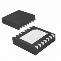
MAX4920BETD+T Maxim Integrated Products, MAX4920BETD+T Datasheet - Page 7

MAX4920BETD+T
Manufacturer Part Number
MAX4920BETD+T
Description
IC CTLR OVP/OCP BATT PWR 14-TDFN
Manufacturer
Maxim Integrated Products
Datasheet
1.MAX4921BETDT.pdf
(19 pages)
Specifications of MAX4920BETD+T
Applications
*
Mounting Type
Surface Mount
Package / Case
14-TDFN Exposed Pad
Lead Free Status / RoHS Status
Lead free / RoHS Compliant
The MAX4919B/MAX4920B have a 4.27V (typ) under-
voltage threshold (UVLO), while the MAX4921B has
2.35V (typ) UVLO threshold. When V
UVLO, GN1 is held low and ACOK is high impedance.
The MAX4919B has a 6.38V (typ) overvoltage threshold
(OVLO), the MAX4920B has a 5.8V (typ) typical OVLO,
and the MAX4921B has a 4.65V (typ) OVLO. When V
is greater than OVLO, GN1 is held low and ACOK is
high impedance.
10, 11
Overvoltage Lockout Thresholds (OVLO)
PIN
4, 5
EP
12
13
14
1
2
3
6
7
8
9
PWR_HOLD Power-Hold Input. Drive PWR_HOLD high to turn on internal pFET.
PWR_ON
HP_PWR
Battery Power-Up Logic with Overvoltage
NAME
ONOK
ACOK
GND
GN1
BTO
GP1
BTI
Undervoltage Lockout (UVLO)
EN
IN
—
_______________________________________________________________________________________
Detailed Description
p-Channel MOSFET Gate-Drive Output. GP1 pulls the external pFET gate down when the input is above
ground.
Voltage Input. IN powers the charge pump required to turn on GN1. When the correct adapter is
plugged in, a one-shot turns on the internal pFET for 1.2s, allowing time for the microprocessor (µP) to
power-up and drive PWR_HOLD high. Bypass IN with a minimum 1µF ceramic capacitor as close as
possible to the device for ±15kV ESD protection. When operating the
MAX4919B/MAX4920B/MAX4921B with an external pFET at GP1, place the 1µF capacitor to GND as
close to the drain of the pFET as possible for the ±15kV ESD protection. If ±15kV ESD protection is not
required, place a minimum 0.1µF capacitor at IN to GND.
n-Channel MOSFET Gate-Drive Output. GN1 is the output of an on-chip charge pump. When V
V
Battery Switch Input. BTI powers the internal circuitry. Bypass BTI with a 0.1µF capacitor. Both BTI
inputs must be externally connected together.
Car-Kit Detection Input. When a car kit is plugged into HP_PWR, a one-shot turns on the internal pFET
for 1.2s, allowing time for the µP to power-up and drive PWR_HOLD high.
Power-On Input. Drive PWR_ON high to turn on the internal pFET. The inverse of the PWR_ON logic
state is represented at the ONOK logic output.
Ground
Open-Drain PWR_ON Indicator Output. ONOK is a logic output with the inverse state of the PWR_ON
input.
Battery Switch Output. Both BTO outputs must be externally connected together.
Open-Drain Adapter Voltage Indicator Output. ACOK pulls low when the adapter voltage is stable
between UVLO and OVLO for 25ms. Connect a pullup resistor from ACOK to a logic supply.
Enable Input. Drive EN low for normal operation. Drive EN high to turn off the external MOSFETs and
enter shutdown mode.
Exposed Paddle. Connect EP to ground.
IN
< V
OVLO
, GN1 is driven above the source voltage to turn on the external n-channel MOSFET.
IN
is less than
and Overcurrent Protection
IN
BTI powers the MAX4919B/MAX4920B/MAX4921B inter-
nal circuitry. BTI also connects internally to a 1.8A (min)
pFET that conducts an external load to the battery using
the BTO output. See the Battery Switchover section.
When the input voltage goes above ground, GP1 pulls
low and turns on the pFET. An internal clamp protects
the pFET by insuring that the GP1 to IN voltage does
not exceed 19.5V when the input (IN) rises to 28V.
FUNCTION
Powering the MAX4919B/
MAX4920B/MAX4921B
Pin Description
GP1 Driver
UVLO
<
7


