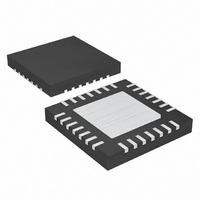
MAX1233ETI+T Maxim Integrated Products, MAX1233ETI+T Datasheet - Page 15

MAX1233ETI+T
Manufacturer Part Number
MAX1233ETI+T
Description
IC CNTRLR TOUCH 28-TQFN
Manufacturer
Maxim Integrated Products
Type
Resistiver
Datasheet
1.MAX1234ETIT.pdf
(44 pages)
Specifications of MAX1233ETI+T
Touch Panel Interface
4-Wire
Number Of Inputs/keys
1, 4 x 4 Keypad
Resolution (bits)
8, 10, 12 b
Data Interface
MICROWIRE™, QSPI™, Serial, SPI™
Data Rate/sampling Rate (sps, Bps)
50k
Voltage Reference
External, Internal
Voltage - Supply
2.7 V ~ 3.6 V
Operating Temperature
-40°C ~ 85°C
Mounting Type
Surface Mount
Package / Case
28-TQFN Exposed Pad
Applications
*
Lead Free Status / RoHS Status
Lead free / RoHS Compliant
measurement of the auxiliary inputs. Figure 4 shows the
on-chip reference circuitry of the MAX1233/MAX1234.
Set the internal reference voltage by writing to the RFV
bits in the ADC control register (see Tables 4, 5, and 12).
The MAX1233/MAX1234 can accept an external refer-
ence connected to REF for ADC conversion.
The MAX1233/MAX1234 can accept an external refer-
ence connected to the REF pin for ADC conversions.
The internal reference should be disabled (RES1 = 1)
when using an external reference. At a conversion rate
of 50ksps, an external reference at REF must deliver up
to 15µA of load current and have 50Ω or less output
impedance. If the external reference has high output
impedance or is noisy, bypass it close to the REF pin
with a 0.1µF capacitor.
Set the type of reference being used by programming
the ADC control register. To select the internal refer-
ence, clock zeros into bits [A/D3:A/D0] and a zero to bit
RES1, as shown in the Control Registers section. To
change to external reference mode, clock zeros into
bits [A/D3:A/D0] and a one to bit RES1. See Table 13
for more information about selecting an internal or
external reference for the ADC.
The MAX1233/MAX1234 are in auto power-down mode
at initial power-up. Set the RES1 and RES0 bits to zero
to use the MAX1233/MAX1234 in the auto power-down
mode. In this mode, the internal reference is normally
off. When a command to perform a battery measure-
Figure 4. Block Diagram of the Internal Reference
Controllers Include DAC and Keypad Controller
BANDGAP
+1.25V
Auto Power-Down Mode (RES1 = RES0 = 0)
Selecting Internal or External Reference
3R
2R
______________________________________________________________________________________
Reference Power Modes
2x
±15kV ESD-Protected Touch-Screen
External Reference
REF PIN
OPTIONAL
ment, temperature measurement, or auxiliary input
measurement is written to the ADC control register, the
device powers on the internal reference, waits for the
internal reference to settle, completes the requested
scan, and powers down the internal reference. The ref-
erence power delay depends upon the ADC resolution
selected (see Table 8). Do not bypass REF with an
external capacitor when performing scans in auto
power-down mode.
In the full-power mode, the RES1 bit is set LOW and
RES0 bit is set HIGH. In this mode, the device is pow-
ered up and the internal ADC reference is always ON.
The MAX1233/MAX1234 internal reference remains fully
powered after completing a scan.
The MAX1233/MAX1234 operate from an internal oscil-
lator, which is accurate to within 20% of the 10MHz
specified clock rate. The internal oscillator controls the
timing of the acquisition, conversion, touch-screen set-
tling, reference power-up, and keypad debounce times.
The MAX1233/MAX1234 have a voltage-output, true 8-bit
monotonic DAC with less than 1LSB integral nonlinearity
error and less than 1LSB differential nonlinearity error. It
requires a supply current of only 150µA (typ) and pro-
vides a buffered voltage output. The DAC is at midscale
code at power-up and remains there until a new code is
written to the DAC register. During shutdown, the DAC’s
output is pulled to ground with a 1MΩ load.
The internal DAC can be used in various system applica-
tions such as LCD/TFT-bias control, automatic tuning
(VCO), power amplifier bias control, programmable
threshold levels, and automatic gain control (AGC).
The 8-bit DAC in the MAX1233/MAX1234 employs a
current-steering topology as shown in Figure 5. At the
core of this DAC is a reference voltage-to-current con-
verter (V/I) that generates a reference current. This cur-
rent is mirrored to 255 equally weighted current
sources. DAC switches control the outputs of these cur-
rent mirrors so that only the desired fraction of the total
current-mirror currents is steered to the DAC output.
The current is then converted to a voltage across a
resistor, and the output amplifier buffers this voltage.
The 8-bit DAC code is binary unipolar with 1LSB =
(V
(0.9 × AV
REF
/256). The DAC has a full-scale output voltage of
DD
- 1LSB).
Full-Power Mode (RES1 = 0, RES0 = 1)
DAC Output Voltage
Internal Clock
8-Bit DAC
15


