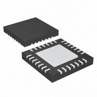
MAX1233ETI+T Maxim Integrated Products, MAX1233ETI+T Datasheet - Page 34

MAX1233ETI+T
Manufacturer Part Number
MAX1233ETI+T
Description
IC CNTRLR TOUCH 28-TQFN
Manufacturer
Maxim Integrated Products
Type
Resistiver
Datasheet
1.MAX1234ETIT.pdf
(44 pages)
Specifications of MAX1233ETI+T
Touch Panel Interface
4-Wire
Number Of Inputs/keys
1, 4 x 4 Keypad
Resolution (bits)
8, 10, 12 b
Data Interface
MICROWIRE™, QSPI™, Serial, SPI™
Data Rate/sampling Rate (sps, Bps)
50k
Voltage Reference
External, Internal
Voltage - Supply
2.7 V ~ 3.6 V
Operating Temperature
-40°C ~ 85°C
Mounting Type
Surface Mount
Package / Case
28-TQFN Exposed Pad
Applications
*
Lead Free Status / RoHS Status
Lead free / RoHS Compliant
±15kV ESD-Protected Touch-Screen
Controllers Include DAC and Keypad Controller
Use this scan to make periodic measurements of both
battery inputs, both auxiliary inputs, and both tempera-
ture inputs. The respective data registers have the lat-
est results at the end of each cycle. Thus, a single write
by the host to the MAX1233/MAX1234 ADC control reg-
ister results in six different measurements being made.
Figure 20 shows this scan operation.
In the touch-initiated screen-scan mode, the
MAX1233/MAX1234 automatically perform a touch-
screen scan upon detecting a screen touch. The touch-
screen scans performed are determined by the
[A/D3:A/D0] written to the ADC control register. Figure
21 shows the flowchart for a complete touch-initiated X-
and Y- coordinate scan. Selection of resolution, conver-
sion rate, averaging, and touch-screen settling time
determine the overall conversion time.
Figure 22 shows the complete flowchart for a touch-
initiated X, Y, and Z scan.
Table 38 shows ADSTS Bit Operation.
In this mode, the host processor decides when a touch-
screen scan begins. The MAX1233/MAX1234 detect a
screen touch and drive PENIRQ LOW. The host recog-
nizes the interrupt request and can choose to write to
the ADC control register to select a touch-screen scan
function (PENSTS = ADSTS = 0). Figures 23 and 24
show the process of a host-initiated screen scan.
In the key-press initiated debounce mode, the
MAX1233/MAX1234 automatically perform a debounce
upon detecting a key press. Key scanning begins once
a key press has been detected and ends when a key
press has been debounced (Figures 25 and 9a).
In this mode, the host processor decides when a
debounce scan begins. The MAX1233/MAX1234 detect
a key press and drive KEYIRQ low. The host processor
recognizes the interrupt request and can choose to
write to the keypad control register to initiate a
debounce scan (Figures 26 and 9b).
Keys are debounced either when (1) a key press has
been detected, or (2) when commanded by the host MPU.
34
______________________________________________________________________________________
Battery Voltage, Auxiliary Input, and
Touch-Initiated Screen Scans
Key-Press Initiated Debounce Scan
Host-Initiated Screen Scans
(PENSTS = 1; ADSTS = 0)
Host-Initiated Debounce Scan
Temperature Input Scan
(KEYSTS1 = 1, KEYSTS0 =0)
(PENSTS = ADSTS = 0)
Keypad Debouncing
The keys scanned by the keypad row and column pins
are debounced for a period of time (debounce period)
as determined by bits [DBN2:DBN0] of the keypad con-
trol register.
The keypad controller continues scanning until the keypad
stays in the same state for an entire debounce period.
Keypad data can be read out of either the keypad data
status register (maskable), or the keypad data pending
register (not maskable). The keypad mask register is
used to mask individual keys in the keypad data status
register.
Write to bits [GP7:GP0] of the GPIO control register to
configure one or more of the R_/C_pins as a GPIO pin.
Write to bits [OE7:OE0] of the GPIO control register to
configure the pins as an input or an output. GPIO data
can be read from or written to the GPIO data register. A
read returns the logic state of the GPIO pin. A write sets
the logic state of a GPIO output pin. Writing to a GPIO
input pin has no effect.
When programmed as GPIO output, by default, the
GPIO pins are active CMOS outputs. Write a 1 to the
pullup disable register to configure the GPIO output as
an open-drain output.
Design Example:
The 8-bit DAC offers the ability to control biasing of
LCD/TFT screens. In the circuit of Figure 27, it is
desired to have the MAX1677 DC-DC converter’s V
to be adjustable.
The minimum and maximum DAC voltages (V
and V
Characteristics table.
The output voltage of the MAX1677 (V
culated by noting the following equations:
Substituting equations 2, 3, and 4 into equation 1
yields:
V
i
i
i
V
(V
1
2
3
OUT
OUT
REFDAC
= i
= V
= (V
DAC(LOW)
2
REFDAC
= V
= V
+ i
REFDAC
3
REFDAC
REFDAC
Using the 8-Bit DAC for LCD/TFT
- V
DAC
) can be found in the Electrical
/ R2
- V
DAC
)
+ i
+ (R1 / R2) V
GPIO Pullup Disable Register
1
R1
) / R3
Contrast Control
REF
OUT
+ (R1 / R3)
[Equation 1]
[Equation 2]
[Equation 3]
[Equation 4]
[Equation 5]
GPIO Control
Keypad Data
) can be cal-
DAC(HIGH)
OUT


