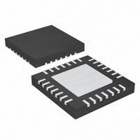
MAX1233ETI+T Maxim Integrated Products, MAX1233ETI+T Datasheet - Page 29

MAX1233ETI+T
Manufacturer Part Number
MAX1233ETI+T
Description
IC CNTRLR TOUCH 28-TQFN
Manufacturer
Maxim Integrated Products
Type
Resistiver
Datasheet
1.MAX1234ETIT.pdf
(44 pages)
Specifications of MAX1233ETI+T
Touch Panel Interface
4-Wire
Number Of Inputs/keys
1, 4 x 4 Keypad
Resolution (bits)
8, 10, 12 b
Data Interface
MICROWIRE™, QSPI™, Serial, SPI™
Data Rate/sampling Rate (sps, Bps)
50k
Voltage Reference
External, Internal
Voltage - Supply
2.7 V ~ 3.6 V
Operating Temperature
-40°C ~ 85°C
Mounting Type
Surface Mount
Package / Case
28-TQFN Exposed Pad
Applications
*
Lead Free Status / RoHS Status
Lead free / RoHS Compliant
The DAC data register stores data that is to be written
to the 8-bit DAC. Table 36 shows the configuration of
the DAC data register. It is right justified with bit 7–bit 0
storing the input data.
Tables 37 and 38 show the format and descriptions for
the GPIO data register. The register is left justified with
data in bit 15–bit 8. Reading the GPIO data register
gives the state of the R_ and C_ pins. Data written to
the GPIO data register appears on those R_ and C_
pins, which are configured as general-purpose outputs.
Data written to pins not configured as general-purpose
outputs is not stored.
The MAX1233/MAX1234 output data is in straight bina-
ry format as shown in Figure 11. This figure shows the
ideal output code for the given input voltage and does
not include the effects of offset error, gain error, noise,
or nonlinearity.
Table 35. Keypad to Key Bit Mapping
Table 36. DAC Data Register(Write 0x000B/Read 0x800B)
Table 37. GPIO Data Register (Write 0x000F/Read 0x800F)
Table 38. GPIO Data Register Bit Descriptions (Write 0x000F/Read 0x800F)
COMPONENT
BIT15 BIT14 BIT13 BIT12 BIT11 BIT10
BIT15 BIT14 BIT13 BIT12 BIT11 BIT10
GPD7
Controllers Include DAC and Keypad Controller
0
15...8
7...0
BIT
R1
R2
R3
R4
GPD6
0
GPD5
GPD7...0
NAME
0
______________________________________________________________________________________
0
C1
K0
K1
K2
K3
GPD4
0
ADC Transfer Function
GPIO data bits for GPIO pins 7...0
Reserved
±15kV ESD-Protected Touch-Screen
C2
K4
K5
K6
K7
GPD3
0
GPIO Data Register
DAC Data Register
GPD2
K10
K11
0
C3
K8
K9
GPD1
BIT9
BIT9
0
K12
K13
K14
K15
C4
GPD0
BIT8
BIT8
0
BIT7
BIT7
DA7
The MAX1233/MAX1234 provide the option of three dif-
ferent resolutions for the ADC: 8, 10, or 12 bits. Lower
resolutions are practical for some measurements such
as touch pressure. Lower resolution conversions have
smaller conversion times and therefore consume less
power. Program the resolution of the MAX1233/
MAX1234 12-bit ADCs by writing to the RES1 and RES0
bits in the ADC control register. When the MAX1233/
MAX1234 power up, both bits are set to zero so the res-
olution is set to 8 bits with a 31µs internally timed refer-
ence power-up delay as indicated by the ADC
resolution control table. As explained in the control reg-
ister section, the RES1 and RES0 bits control the refer-
Figure 11. Ideal Input Voltages and Output Codes
0
DESCRIPTION
Programmable 8-/10-/12-Bit Resolution
BIT6
BIT6
DA6
11 ... 111
11 ... 110
11 ... 101
00 ... 011
00 ... 010
00 ... 001
00 ... 000
0
OUTPUT CODE
0
BIT5
BIT5
DA5
0
Applications Information
1
INPUT VOLTAGE (LSB)
2
BIT4
BIT4
DA4
3
0
FULL-SCALE
TRANSITION
BIT3
BIT3
DA3
0
BIT2
BIT2
DA2
FS - 3/2LSB
0
MAX1233
MAX1234
FS = V
ZS = GND
1LSB = V
BIT1
BIT1
DA1
FS
0
REF
4096
REF
BIT0
BIT0
DA0
0
29


