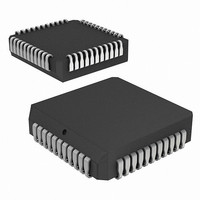
CY7C9235A-270JXC Cypress Semiconductor Corp, CY7C9235A-270JXC Datasheet - Page 3

CY7C9235A-270JXC
Manufacturer Part Number
CY7C9235A-270JXC
Description
IC SMPTE ENCODER 44-PLCC
Manufacturer
Cypress Semiconductor Corp
Datasheet
1.CY7C9235A-270JXC.pdf
(8 pages)
Specifications of CY7C9235A-270JXC
Applications
*
Mounting Type
Surface Mount
Package / Case
44-PLCC
Lead Free Status / RoHS Status
Lead free / RoHS Compliant
Available stocks
Company
Part Number
Manufacturer
Quantity
Price
Company:
Part Number:
CY7C9235A-270JXC
Manufacturer:
Cypress Semiconductor Corp
Quantity:
10 000
Document #: 38-02082 Rev. **
Pin Descriptions
SC/D_EN
PD
PD
PD
Q
Q
Q
DVB_EN
CKW
ENA_OUT
OE
V
V
CC
SS
9
8–1
0
(SVS)
(SC/D)
9
8–1
0
Name
(SVS)
(SC/D)
Input
Input
Input
Input
Output
Output
Output
Input
Input
Output
Input
I/O
CY7C9235A SMPTE-259M Encoder (continued)
Special Character/Data Select Enable. This input is only valid when DVB_EN is active (LOW). If
SC/D_EN is HIGH and a HIGH input is present on PD
cycle, forcing the CY7B9234 serializer to generate an 8B/10B control character as selected by the
character present on the PD
Q
Parallel Data 9 or Send Violation Symbol. This is the MSB of the input data field. It is latched in
the input register at the rising edge of CKW. When DVB_EN is active (LOW) and SVS_EN is HIGH,
this latched input is routed to the output register bit Q
SVS_EN is LOW, output register bit Q
inactive (HIGH), this latched input is routed to the scrambler and NRZI encoder.
Parallel Data 8 through 1. The signals present at the PD
at the rising edge of CKW. When DVB_EN is HIGH, these signals are the middle eight bits of the
SMPTE 10-bit data field, and are then routed to the scrambler and NRZI encoder. When DVB_EN
is active (LOW), these signals are full DVB-ASI data bus, and are then routed to the Q
Parallel Data 0 or Special Code/Data Select. This is the LSB of the input data field. It is latched in
the input register at the rising edge of CKW. When DVB_EN is active (LOW) and SC/D_EN is HIGH,
this input is routed to output register bit Q
LOW, output register bit Q
this input data bit is routed through the input register and the scrambler and NRZI encoder.
Output Bit 9. This is the MSB of the output register. It should be connected directly to the CY7B9234
serializer input signal SVS(Dj).
Output Bits 8 through 1. These signals should be connected directly to the CY7B9234 serializer
input signals D
Output Bit 0. This is the LSB of the output register. It should be connected directly to the CY7B9234
serializer input signal SC/D(Da).
DVB Mode Enable. This signal is sampled by the rising edge of the CKW clock. If DVB_EN is active
(LOW), the data present on the PD
ENA_OUT outputs.
Clock Write. This clock controls all synchronous operations of the CY7C9235A. It operates at the
character rate which is equivalent to one tenth the serialized bit-rate. This clock also connects directly
to the CKW input of the CY7B9234 serializer.
Enable Parallel Data Out. This output attached directly to the CY7B9234 ENA input, and identifies
when valid data is available at the CY7C9235A outputs. If used only for SMPTE-259M data streams,
this output may be left open, with the ENA input to the CY7B9234 directly connected to V
Output Enable. When this signal is HIGH all outputs are driven to their normal logic levels. When
LOW, all outputs are placed in a High-Z state.
Power.
Ground.
0
is forced to a LOW (data only) state.
7 0
respectively.
0
(SC/D) is forced to a LOW (zero) level. When DVB_EN is inactive (HIGH),
8–1
inputs. If SC/D_EN is LOW, the level present on PD
0 9
, ENA, and ENN inputs are latched and routed to the Q
9
(SVS) is forced to a LOW (zero) level. When DVB_EN is
0
(SVS). When DVB_EN is active (LOW) and SC/D_EN is
Description
9
0
(SVS). When DVB_EN is active (LOW) and
, Q
8–1
0
will also be high on a following clock
inputs are latched in the input register
CY7C9235A
0
is ignored and
8 1
Page 3 of 8
SS
outputs.
0 9
.
and


