CY7C9235A-270JXC Cypress Semiconductor Corp, CY7C9235A-270JXC Datasheet - Page 5
CY7C9235A-270JXC
Manufacturer Part Number
CY7C9235A-270JXC
Description
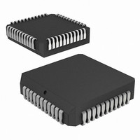
IC SMPTE ENCODER 44-PLCC
Manufacturer
Cypress Semiconductor Corp
Datasheet
1.CY7C9235A-270JXC.pdf
(8 pages)
Specifications of CY7C9235A-270JXC
Applications
*
Mounting Type
Surface Mount
Package / Case
44-PLCC
Lead Free Status / RoHS Status
Lead free / RoHS Compliant
Available stocks
Company
Part Number
Manufacturer
Quantity
Price
Company:

Part Number:
CY7C9235A-270JXC
Manufacturer:
Cypress Semiconductor Corp
Quantity:
10 000


Document #: 38-02082 Rev. **
Maximum Ratings
(Above which the useful life may be impaired. For user guide-
lines, not tested.)
Storage Temperature
Supply Voltage to Ground Potential
DC Voltage Applied to Outputs
in High-Z State
Output Current into Outputs.........................................16 mA
Electrical Characteristics
Capacitance
AC Test Loads and Waveforms
Notes:
V
V
V
V
I
I
I
C
C
C
1. Single Power Supply: The voltage on any input or I/O pin cannot exceed the power pin during power-up.
2. These are absolute values with respect to device ground. All overshoots due to system or tester noise are included.
3. Not more than one output should be tested at a time. Duration of the short circuit should not exceed 1 second. V
4. Tested initially and after any design or process changes that may affect these parameters.
IX
OZ
OS
Parameter
OH
OL
IH
IL
IN
OUT
CLK
caused by tester ground degradation.
Parameter
OUTPUT
Equivalent to:
INCLUDING
JIG AND
SCOPE
Output HIGH Voltage
Output LOW Voltage
Input HIGH Voltage
Input LOW Voltage
Input Load Current
Output Leakage Current
Output Short Circuit Current
5V
[4]
OUTPUT
35 pF
[1]
(a)
THÉVENIN EQUIVALENT
Description
238
Input Capacitance
Output Capacitance
Clock Signal Capacitance
5 OR 35 pF
99
Over the Operating Range
170
Description
2.08V
[3,4]
40°C to +125°C
OUTPUT
0.5V to +7.0V
0.5V to +7.0V
INCLUDING
JIG AND
SCOPE
5V
V
V
Guaranteed Input Logical HIGH
Voltage for all Inputs
Guaranteed Input Logical LOW
Voltage for all Inputs
V
V
V
CC
CC
I
O
CC
= V
= V
=Min., I
=Min., I
= Max., V
5 pF
V
V
V
CC
CC
IN
IN
IN
(b)
or V
= 5.0V at f = 1 MHz
= 5.0V at f = 1 MHz
= 5.0V at f = 1 MHz
or V
238
OH
OL
Test Conditions
SS
Test Conditions
DC Input Voltage
Static Discharge Voltage
(per MIL-STD-883, Method 3015)
DC Input Current
Latch-up Current
Operating Range
SS
OUT
= 16.0 mA
Commercial
= 3.2 mA
= 0.5V
Range
170
[2]
[2]
GND
5.0V
Ambient Temperature
<2 ns
OUT
0°C to +70°C
= 0.5V has been chosen to avoid test problems
ALL INPUT PULSES
Min.
–0.5
10%
2.4
2.0
Max.
10
50
30
10
12
12
90%
(c)
CY7C9235A
Max.
+10
+50
0.5
7.0
0.8
160
0.5V to +7.0V
90%
5V
Page 5 of 8
10%
Unit
V
pF
pF
pF
<2 ns
CC
200 mA
2001 V
5%
20 mA
Unit
mA
V
V
V
V
A
A
Related parts for CY7C9235A-270JXC
Image
Part Number
Description
Manufacturer
Datasheet
Request
R

Part Number:
Description:
Manufacturer:
Cypress Semiconductor Corp
Datasheet:
Part Number:
Description:
Manufacturer:
Cypress Semiconductor Corp
Datasheet:
Part Number:
Description:
Manufacturer:
Cypress Semiconductor Corp
Datasheet:
Part Number:
Description:
Manufacturer:
Cypress Semiconductor Corp
Datasheet:
Part Number:
Description:
Manufacturer:
Cypress Semiconductor Corp
Datasheet:
Part Number:
Description:
Manufacturer:
Cypress Semiconductor Corp
Datasheet: