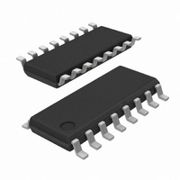
SI8405AA-B-IS1 Silicon Laboratories Inc, SI8405AA-B-IS1 Datasheet - Page 17

SI8405AA-B-IS1
Manufacturer Part Number
SI8405AA-B-IS1
Description
IC ISOLATOR BIDIR I2C 16-SOIC
Manufacturer
Silicon Laboratories Inc
Datasheet
1.SI8401AA-B-ISR.pdf
(34 pages)
Specifications of SI8405AA-B-IS1
Number Of Channels
6
Package / Case
16-SOIC (3.9mm Width)
Inputs - Side 1/side 2
3/3
Isolation Rating
1000Vrms
Voltage - Supply
3 V ~ 5.5 V
Data Rate
10Mbps
Output Type
Open Drain
Operating Temperature
-40°C ~ 125°C
Mounting Style
SMD/SMT
Propagation Delay Time
20 ns
Supply Voltage (max)
5.5 V
Supply Voltage (min)
3 V
Supply Current
6.2 mA
Maximum Operating Temperature
+ 125 C
Minimum Operating Temperature
- 40 C
Lead Free Status / RoHS Status
Lead free / RoHS Compliant
Propagation Delay
-
Lead Free Status / Rohs Status
Lead free / RoHS Compliant
Si840x
4. Layout Recommendations
To ensure safety in the end user application, high voltage circuits (i.e., circuits with >30 V
) must be physically
AC
separated from the safety extra-low voltage circuits (SELV is a circuit with <30 V
) by a certain distance
AC
(creepage/clearance). If a component, such as a digital isolator, straddles this isolation barrier, it must meet those
creepage/clearance requirements and also provide a sufficiently large high-voltage breakdown protection rating
(commonly referred to as working voltage protection). Table 6 on page 9 and Table 7 on page 9 detail the working
voltage and creepage/clearance capabilities of the Si84xx. These tables also detail the component standards
(UL1577, IEC60747, CSA 5A), which are readily accepted by certification bodies to provide proof for end-system
specifications requirements. Refer to the end-system specification (61010-1, 60950-1, etc.) requirements before
starting any design that uses a digital isolator.
4.1. Supply Bypass
The Si84xx family requires a 1 µF bypass capacitor between AVDD and AGND and BVDD and BGND. The
capacitor should be placed as close as possible to the package. To enhance the robustness of a design, it is further
recommended that the user also add 1 µF bypass capacitors and include 100 resistors in series with the inputs,
outputs, and supply pins if the system is excessively noisy. See "6.Errata and Design Migration Guidelines" on
page 22 for more details.
4.2. Pin Connections
No connect pins are not internally connected. They can be left floating, tied to
, or tied to GND.
V
DD
4.3. Output Pin Termination
C isolator channel is approximately 85 , ±40%, which is a combination
2
The nominal output impedance of an non-I
of the value of the on-chip series termination resistor and channel resistance of the output driver FET. When driving
loads where transmission line effects will be a factor, output pins should be appropriately terminated with controlled
impedance PCB traces.
Rev. 1.3
17


