6N139-000E Avago Technologies US Inc., 6N139-000E Datasheet
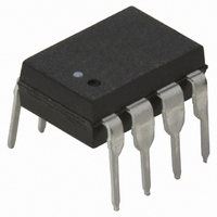
OPTOCOUPLER DARL-OUT 8-DIP

6N139-000E

Manufacturer Part Number
6N139-000E
Description
OPTOCOUPLER DARL-OUT 8-DIP
Manufacturer
Avago Technologies US Inc.
Type
Analogr
Datasheets

Specifications of 6N139-000E

Input Type
DC
Package / Case
8-DIP (0.300", 7.62mm)
Voltage - Isolation
3750Vrms
Number Of Channels
1, Unidirectional
Current - Output / Channel
60mA
Data Rate
100KBd
Propagation Delay High - Low @ If
5µs @ 500µA
Current - Dc Forward (if)
20mA
Output Type
Open Collector
Mounting Type
Through Hole
Isolation Voltage
3750 Vrms
Maximum Fall Time
25 us
Maximum Rise Time
60 us
Minimum Forward Diode Voltage
1.25 V
Output Device
Darlington With Base
Configuration
1 Channel
Current Transfer Ratio
5000 %
Maximum Baud Rate
100 KBps
Maximum Forward Diode Voltage
1.7 V
Maximum Reverse Diode Voltage
5 V
Maximum Input Diode Current
20 mA
Maximum Power Dissipation
135 mW
Maximum Operating Temperature
+ 70 C
Minimum Operating Temperature
0 C
Package Type
8-Pin DIP
No. Of Channels
1
Optocoupler Output Type
Photodarlington
Input Current
12mA
Output Voltage
18V
Opto Case Style
DIP
No. Of Pins
8
Ctr Max
5000%
Ctr Min
400%
Rohs Compliant
Yes
Lead Free Status / RoHS Status
Lead free / RoHS Compliant
Lead Free Status / RoHS Status
Lead free / RoHS Compliant, Lead free / RoHS Compliant
Other names
516-1601-5

Available stocks

Company
Part Number
Manufacturer
Quantity
Price
Part Number:
6N139-000E
Manufacturer:
AVG
Quantity:
4 684
Part Number:
6N139-000E
Manufacturer:
AVAGO/安华高
Quantity:
20 000
Hermetically Sealed, Low I
High Gain Optocouplers
Data Sheet
6N140A,* HCPL-675X, 83024, HCPL-570X, HCPL-177K, 5962-89810,
HCPL-573X, HCPL-673X, 5962-89785, 5962-98002
*See matrix for available extensions.
Description
These units are single, dual, and quad channel, hermeti-
cally sealed optocoup lers. The products are capable of
operation and storage over the full military temperature
range and can be purchased as either standard product or
with full MIL-PRF-38534 Class Level H or K testing or from
the appro priate DSCC Drawing. All devices are manufac-
tured and tested on a MIL-PRF-38534 certified line and are
included in the DSCC Quali fied Manufacturers List QML-
38534 for Hybrid Microcircuits.
Each channel contains a GaAsP light emitting diode which
is optically coupled to an integrated high gain photon
detector. The high gain output stage features an open
collector output providing both lower saturation voltage
and higher signaling speed than possible with conven-
tional photo-Darling ton optocouplers. The shallow depth
and small junctions offered by the IC process provides
better radiation immunity than conven tional photo tran-
sistor optocouplers.
The supply voltage can be operated as low as 2.0 V without
adversely affecting the parametric performance.
These devices have a 300% minimum CTR at an input
current of only 0.5 mA making them ideal for use in low
input current applications such as MOS, CMOS, low power
logic interfaces or line receivers. Compatibility with high
voltage CMOS logic systems is assured by specifying I
and I
OH
at 18 Volts.
CAUTION: It is advised that normal static precautions be taken in handling and assembly
of this component to prevent damage and/or degradation which may be induced by ESD.
The connection of a 0.1 µ F bypass capacitor between V
F
, Wide V
CC
,
CCH
Features
• Dual marked with device part number and DSCC
• Manufactured and tested on a MIL-PRF-38534 Certified
• QML-38534, Class H and K
• Five hermetically sealed package configurations
• Performance guaranteed over full military temperature
• Low input current requirement: 0.5 mA
• High current transfer ratio: 1500% typical @ I
• Low output saturation voltage: 0.11 V typical
• 1500 Vdc withstand test voltage
• High radiation immunity
• 6N138/9, HCPL-2730/31 function compatibility
• Reliability data
Applications
• Military and aerospace
• High reliability systems
• Telephone ring detection
• Microprocessor system interface
• Transportation, medical, and life critical systems
• Isolated input line receiver
• EIA RS-232-C line receiver
• Voltage level shifting
• Isolated input line receiver
• Isolated output line driver
• Logic ground isolation
• Harsh industrial environments
• Current loop receiver
• System test equipment isolation
• Process control input/output isolation
drawing number
Line
range: -55°C to +125°C
CC
and GND is recommended.
F
= 0.5 mA

Related parts for 6N139-000E

6N139-000E Summary of contents

Page 1

Hermetically Sealed, Low I High Gain Optocouplers Data Sheet 6N140A,* HCPL-675X, 83024, HCPL-570X, HCPL-177K, 5962-89810, HCPL-573X, HCPL-673X, 5962-89785, 5962-98002 *See matrix for available extensions. Description These units are single, dual, and quad channel, hermeti- cally sealed optocoup lers. The products ...

Page 2

Functional Diagram Multiple Channel Devices Available Truth Table (Positive Logic) Input Output On (H) L Off (L) H Selection Guide-Package Styles and Lead Configuration Options Package 16 pin DIP Lead Style Through ...

Page 3

Functional Diagrams 16 pin DIP 8 pin DIP Through Hole Through Hole 4 Channels 1 Channel Note: All DIP and ...

Page 4

Outline Drawings (continued) 16 Pin Flat Pack, 4 Channels 7.24 (0.285) 6.99 (0.275) 11.13 (0.438) 10.72 (0.422) 8.13 (0.320) 2.85 (0.112) MAX. 0.89 (0.035) 0.69 (0.027) (0.206) Note: Dimensions in Millimeters (Inches) 20 Terminal LCCC Surface Mount, 2 Channels 8.70 ...

Page 5

Hermetic Optocoupler Options Option Description 100 Surface mountable hermetic optocoupler with leads trimmed for butt joint assembly. This option is available on com- mercial and hi-rel product in 8 and 16 pin DIP (see drawings below for details). 0.51 (0.020) ...

Page 6

Absolute Maximum Ratings Parameter Storage Temperature Operating Temperature Case Temperature Junction Temperature Lead Solder Temperature Output Current (each channel) Output Voltage (each channel) Supply Voltage Output Power Dissipation (each channel) Peak Input Current (each channel, <1 ms duration) Average Input ...

Page 7

Electrical Characteristics -55°C to +125°C, unless otherwise specified A Parameter Symbol Test Conditions Current Transfer CTR 0.5 mA Ratio 1 ...

Page 8

Electrical Characteristics (cont -55°C to +125°C, unless otherwise specified A Parameter Symbol Test Conditions Propagation Delay 0.5 mA, R PHL F Time to Logic Low Output ...

Page 9

Notes: 1. GND Pin should be the most negative voltage at the detector side. Keeping V as low as possible, but greater than 2.0 V, will provide CC lowest total I over temperature Output power is collector output ...

Page 10

Figure 1. Input Diode Forward Current vs. Forward Voltage. Figure 4. Normalized Supply Current vs. Input Diode Forward Current. Figure 7. Propagation Delay vs. Input Diode Forward Current. 10 Figure 2. Normalized DC Transfer Characteristics. Figure 5. Propagation Delay to ...

Page 11

PULSE GEN  100 0.5ms 8 PULSE MONITOR SEE ...

Page 12

MIL-PRF-38534 Class H, Class K, and DSCC SMD Test Program Avago’s Hi-Rel Optocouplers are in compliance with MIL- PRF-38534 Class H and K. Class H and Class K devices are also in compliance with DSCC drawings 83024, 5962- 89785, 5962-89810, ...

Related keywords