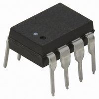
6N139-000E Avago Technologies US Inc., 6N139-000E Datasheet

6N139-000E
Specifications of 6N139-000E
Available stocks
Related parts for 6N139-000E
6N139-000E Summary of contents
Page 1
... A base access terminal allows a gain bandwidth adjustment to be made. The 6N139, HCPL-0701, and CNW139 are for use in CMOS, LSTTL or other low power applications. A 400% mini- mum current transfer ratio is guaranteed over 0 to 70°C operating range for only 0 LED current. ...
Page 2
... The Selection Guide 8-Pin DIP (300 Mil) Small Outline SO-8 Dual Single Single Channel Channel Channel Package Package Package HCPL- HCPL- 6N139 2731 0701 [1] 6N138 2730 0700 [1] HCPL-4701 4731 070A [1] [1] Note: 1. Technical data are on separate Avago publications. 2 lead profile is designed to be compatible with standard surface mount processes ...
Page 3
... Ordering Information 6N138, 6N139, HCPL-0700 and HCPL-0701 are UL Recognized with 3750 Vrms for 1 minute per UL1577 and are approved under CSA Component Acceptance Notice #5, File CA 88324. Option Part RoHS non RoHS Number Compliant Compliant Package -000E no option 300 mil DIP-8 -300E ...
Page 4
... TYPE NUMBER A XXXXZ YYWW 1.19 (0.047) MAX. 3.56 ± 0.13 (0.140 ± 0.005) 1.080 ± 0.320 (0.043 ± 0.013) **JEDEC Registered Data. 8-Pin DIP Package with Gull Wing Surface Mount Option 300 (6N139/6N138) 9.65 ± 0.25 (0.380 ± 0.010 1.19 (0.047) MAX. ...
Page 5
Small Outline SO-8 Package (HCPL-0701/HCPL-0700 3.937 ± 0.127 (0.155 ± 0.005 PIN ONE 0.406 ± 0.076 (0.016 ± 0.003) * 5.080 ± 0.127 (0.200 ± 0.005) 3.175 ± 0.127 (0.125 ± 0.005) * TOTAL PACKAGE LENGTH ...
Page 6
Widebody DIP Package with Gull Wing Surface Mount Option 300 (HCNW139/HCNW138) 11.15 ± 0.15 (0.442 ± 0.006 1.78 ± 0.15 (0.070 ± 0.006) 2.54 (0.100) BSC DIMENSIONS IN MILLIMETERS (INCHES). LEAD COPLANARITY = ...
Page 7
... PREHEAT 60 to 180 SEC °C to PEAK TIME Regulatory Information The 6N139/138, HCNW139/138, and HCPL-0701/0700 have been approved by the following organizations: UL Recognized under UL 1577, Component Recognition Program, File E55361. CSA Approved under CSA Component Acceptance Notice #5, File CA 88324. Insulation and Safety Related Specifications ...
Page 8
IEC/EN/DIN EN 60747-5-2 Insulation Related Characteristics (HCNW139 and HCNW138) Description Installation Classification per DIN VDE 0110/1.89, Table 1 for rated mains voltage ≤600 V rms for rated mains voltage ≤1000 V rms Climatic Classification Pollution Degree (DIN VDE 0110/1.89) Maximum ...
Page 9
... Output Power Dissipation Total Power Dissipation Lead Solder Temperature (for Through Hole Devices) Reflow Temperature Profile (for SOIC-8 and Option #300) *JEDEC Registered Data for 6N139 and 6N138. **0°C to 70°C on JEDEC Registration. Recommended Operating Conditions Parameter Power Supply Voltage Forward Input Current (ON) ...
Page 10
... HCNW138 Temperature ∆V F Coefficient of ∆T A Forward Voltage Input C IN Capacitance HCNW139 HCNW138 *JEDEC Registered Data for 6N139 and 6N138. **All typical values 25°C and unless otherwise noted ≤ ≤ V ≤ 0.8 V, unless otherwise specified. F(ON) F(OFF) Min. Typ.** Max. Units ...
Page 11
... HCPL-0700 HCNW138 Common Mode | Transient Immunity at Logic High Output Common Mode | Transient Immunity at Logic Low Output *JEDEC Registered Data for 6N139 and 6N138. **All typical values 25°C and unless otherwise noted 70°C unless otherwise specified Min. Typ.** Max. T =25° 25 ...
Page 12
Package Characteristics Parameter Input-Output Momentary Withstand Voltage† Option 020 HCNW139 HCNW138 Resistance (Input-Output) Capacitance (Input-Output) **All typicals 25°C, unless otherwise noted. A †The Input-Output Momentary Withstand Voltage is a dielectric voltage rating that should not be interpreted ...
Page 13
... TEMPERATURE – °C A Figure 8. Forward voltage vs. temperature 6N139 Figure 8 100 85° 1 70° 25° 0 0° -40° 0.01 0.01 0 – INPUT DIODE FORWARD CURRENT – Figure 3. 6N138/6N139 output current vs. input diode forward current 6N139 fig 1 2.2 kΩ µs t PLH PHL 0 100 -60 -40 - ...
Page 14
... DUTY CYCLE 1.5 V I/f < 100 µ MONITOR F t PLH 6N139 Figure 6N139 Figure 13 www.avagotech.com WIDEBODY P (mW (mA 100 125 150 175 T – CASE TEMPERATURE – °C S 6N139 fig 11b 0.1 µ INCLUDES PROBE AND FIXTURE CAPACITANCE R (SEE NOTE – PULSE GEN pF* L ...


