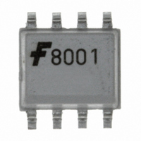
FOD8001 Fairchild Optoelectronics Group, FOD8001 Datasheet - Page 2

FOD8001
Manufacturer Part Number
FOD8001
Description
OPTOCOUPLER 3.3V 8-SOIC
Manufacturer
Fairchild Optoelectronics Group
Series
OPTOPLANAR®r
Datasheet
1.FOD8001R2.pdf
(12 pages)
Specifications of FOD8001
Voltage - Isolation
3750Vrms
Number Of Channels
1, Unidirectional
Current - Output / Channel
10mA
Data Rate
25Mbps
Propagation Delay High - Low @ If
25ns
Input Type
Logic
Output Type
Push-Pull, Totem-Pole
Mounting Type
Surface Mount
Package / Case
8-SOIC (0.154", 3.90mm Width)
Lead Free Status / RoHS Status
Lead free / RoHS Compliant
©2008 Fairchild Semiconductor Corporation
FOD8001 Rev. 1.0.3
Pin Definitions
Absolute Maximum Ratings
Stresses exceeding the absolute maximum ratings may damage the device. The device may not function or be
operable above the recommended operating conditions and stressing the parts to these levels is not recommended.
In addition, extended exposure to stresses above the recommended operating conditions may affect device reliability.
The absolute maximum ratings are stress ratings only.
Recommended Operating Conditions
The Recommended Operating Conditions table defines the conditions for actual device operation. Recommended
operating conditions are specified to ensure optimal performance to the datasheet specifications. Fairchild does not
recommend exceeding them or designing to absolute maximum ratings.
Notes:
1. Derate linearly from 25°C at a rate of tbd W/°C
2. Derate linearly from 25°C at a rate of tbd mW/°C.
3. Functional operation under these conditions is not implied. Permanent damage may occur if the device is subjected
4. 0.1µF bypass capacitor must be connected between Pin 1 and 4, and 5 and 8.
V
to conditions outside these ratings.
Pin Number
Symbol
DD1
V
Symbol
t
V
DD1
V
T
r
, V
, t
IH
A
IL
T
T
T
PD
PD
V
f
1
2
3
4
5
6
7
8
OPR
STG
SOL
V
I
DD2
, V
I
O
I
O
I
O
I
DD2
Ambient Operating Temperature
Supply Voltages (3.3V Operation)
Supply Voltages (5.0V Operation)
Logic High Input Voltage
Logic Low Input Voltage
Input Signal Rise and Fall Time
Storage Temperature
Operating Temperature
Lead Solder Temperature
(Refer to Reflow Temperature Profile)
Supply Voltage
Input Voltage
Input DC Current
Output Voltage
Average Output Current
Input Power Dissipation
Total Power Dissipation
Pin Name
GND1
GND2
V
V
NC
V
DD1
DD2
V
O
I
Parameter
(T
Parameter
Input Supply Voltage
Input Data
LED Anode – Must be left unconnected
Input Ground
Output Ground
Output Data
Not Connected
Output Supply Voltage
A
= 25°C Unless otherwise specified.)
(2)(3)
(1)(3)
(4)
(4)
2
Pin Function Description
Min.
-40
3.0
4.5
2.0
0
-0.5 to V
-0.5 to V
260 for 10 sec
-40 to +125
-40 to +105
-10 to +10
0 to 6.0
Value
90
70
10
DD1
DD2
+ 0.5
+ 0.5
Max.
+105
V
3.6
5.5
0.8
1.0
DD
Units
www.fairchildsemi.com
mW
mW
mA
°C
°C
°C
µA
V
V
V
Unit
ms
°C
V
V
V


