TCET4100 Vishay, TCET4100 Datasheet - Page 3
TCET4100
Manufacturer Part Number
TCET4100
Description
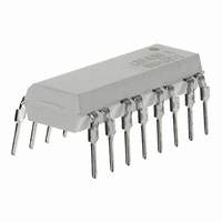
OPTOCP PHOTOTRANS 4CH 600% 16DIP
Manufacturer
Vishay
Datasheet
1.TCET4100.pdf
(9 pages)
Specifications of TCET4100
Mounting Type
Through Hole
Isolation Voltage
5000 Vrms
Number Of Channels
4
Input Type
DC
Voltage - Isolation
5000Vrms
Current Transfer Ratio (min)
50% @ 5mA
Current Transfer Ratio (max)
600% @ 5mA
Voltage - Output
70V
Current - Output / Channel
50mA
Current - Dc Forward (if)
60mA
Vce Saturation (max)
300mV
Output Type
Transistor
Package / Case
16-DIP (0.300", 7.62mm)
Maximum Input Diode Current
60 mA
Maximum Reverse Diode Voltage
6 V
Output Device
Transistor
Configuration
4
Maximum Collector Emitter Voltage
70 V
Maximum Collector Emitter Saturation Voltage
300 mV
Current Transfer Ratio
600 %
Maximum Forward Diode Voltage
1.6 V
Maximum Collector Current
50 mA
Maximum Power Dissipation
265 mW
Maximum Operating Temperature
+ 100 C
Minimum Operating Temperature
- 40 C
No. Of Channels
4
Optocoupler Output Type
Phototransistor
Input Current
50mA
Output Voltage
70V
Opto Case Style
DIP
No. Of Pins
16
Lead Free Status / RoHS Status
Lead free / RoHS Compliant
Lead Free Status / RoHS Status
Lead free / RoHS Compliant, Lead free / RoHS Compliant
Other names
751-1371-5
TCET4100
TCET4100


Coupler
Current Transfer Ratio
Maximum Safety Ratings
(according to DIN EN 60747-5-2(VDE0884)/ DIN EN 60747-5-5 pending) see figure 1
Input
Output
Coupler
Insulation Rated Parameters
Document Number 83727
Rev. 1.4, 26-Oct-04
This optocoupler is suitable for safe electrical isolation only within the safety ratings.
Compliance with the safety ratings shall be ensured by means of suitable protective circuits.
Collector emitter saturation
voltage
Cut-off frequency
Coupling capacitance
I
Forward current
Power dissipation
Rated impulse voltage
Safety temperature
Partial discharge test voltage -
Routine test
Partial discharge test voltage -
Lot test (sample test)
Insulation resistance
C
/I
F
Parameter
Parameter
Parameter
Parameter
Parameter
Parameter
I
V
R
f = 1 MHz
V
100 %, t
t
(see figure 2)
V
V
V
(construction test only)
F
Tr
CE
CE
IO
IO
IO
L
= 10 mA, I
= 60 s, t
= 100 Ω
= 500 V
= 500 V, T
= 500 V, T
= 5 V, I
= 5 V, I
test
Test condition
Test condition
Test condition
Test condition
Test condition
Test condition
test
F
F
= 1 s
C
= 10 mA,
= 5 mA
= 10 s,
amb
amb
= 1 mA
= 100 °C
= 150 °C
Symbol
Symbol
Symbol
Symbol
Symbol
Symbol
V
V
V
P
CTR
CEsat
V
V
R
R
R
IOTM
IOTM
C
T
f
I
diss
F
pd
pd
c
IO
IO
IO
si
k
TCET2100 / TCET4100
10
10
Min
Min
Min
Min
Min
Min
10
1.6
1.3
50
8
12
11
9
Vishay Semiconductors
Typ.
110
Typ.
Typ.
Typ.
Typ.
Typ.
0.3
Max
Max
Max
Max
Max
Max
600
130
265
150
0.3
8
www.vishay.com
Unit
kHz
Unit
Unit
Unit
mW
Unit
Unit
mA
pF
kV
kV
kV
kV
°C
%
Ω
Ω
Ω
V
3
Related parts for TCET4100
Image
Part Number
Description
Manufacturer
Datasheet
Request
R

Part Number:
Description:
357-036-542-201 CARDEDGE 36POS DL .156 BLK LOPRO
Manufacturer:
Vishay
Datasheet:
Part Number:
Description:
357-036-542-201 CARDEDGE 36POS DL .156 BLK LOPRO
Manufacturer:
Vishay
Datasheet:
Part Number:
Description:
357-036-542-201 CARDEDGE 36POS DL .156 BLK LOPRO
Manufacturer:
Vishay
Datasheet:
Part Number:
Description:
357-036-542-201 CARDEDGE 36POS DL .156 BLK LOPRO
Manufacturer:
Vishay
Datasheet:
Part Number:
Description:
357-036-542-201 CARDEDGE 36POS DL .156 BLK LOPRO
Manufacturer:
Vishay
Datasheet:
Part Number:
Description:
357-036-542-201 CARDEDGE 36POS DL .156 BLK LOPRO
Manufacturer:
Vishay
Datasheet:
Part Number:
Description:
357-036-542-201 CARDEDGE 36POS DL .156 BLK LOPRO
Manufacturer:
Vishay
Datasheet:
Part Number:
Description:
357-036-542-201 CARDEDGE 36POS DL .156 BLK LOPRO
Manufacturer:
Vishay
Datasheet:
Part Number:
Description:
357-036-542-201 CARDEDGE 36POS DL .156 BLK LOPRO
Manufacturer:
Vishay
Datasheet:
Part Number:
Description:
357-036-542-201 CARDEDGE 36POS DL .156 BLK LOPRO
Manufacturer:
Vishay
Datasheet:
Part Number:
Description:
357-036-542-201 CARDEDGE 36POS DL .156 BLK LOPRO
Manufacturer:
Vishay
Datasheet:
Part Number:
Description:
357-036-542-201 CARDEDGE 36POS DL .156 BLK LOPRO
Manufacturer:
Vishay
Datasheet:
Part Number:
Description:
357-036-542-201 CARDEDGE 36POS DL .156 BLK LOPRO
Manufacturer:
Vishay
Datasheet:
Part Number:
Description:
357-036-542-201 CARDEDGE 36POS DL .156 BLK LOPRO
Manufacturer:
Vishay
Datasheet:
Part Number:
Description:
357-036-542-201 CARDEDGE 36POS DL .156 BLK LOPRO
Manufacturer:
Vishay
Datasheet: