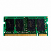
MT16VDDF12864HY-40BD2 Micron Technology Inc, MT16VDDF12864HY-40BD2 Datasheet - Page 14

MT16VDDF12864HY-40BD2
Manufacturer Part Number
MT16VDDF12864HY-40BD2
Description
MODULE SDRAM DDR 1GB 200SODIMM
Manufacturer
Micron Technology Inc
Datasheet
1.MT16VDDF12864HY-40BF2.pdf
(29 pages)
Specifications of MT16VDDF12864HY-40BD2
Memory Type
DDR SDRAM
Memory Size
1GB
Speed
400MT/s
Package / Case
200-SODIMM
Lead Free Status / RoHS Status
Lead free / RoHS Compliant
Table 12: I
Notes: 1–5, 8, 10, 12, 47; DDR SDRAM devices only; notes appear on pages 18–20; 0°C
pdf: 09005aef80b57837, source: 09005aef80b577fa
DDAF16C64_128x64HG.fm - Rev. D 9/04 EN
PARAMETER/CONDITION
OPERATING CURRENT: One device bank; Active-Precharge;
(MIN);
Address and control inputs changing once every two clock cycles
OPERATING CURRENT: One device bank; Active-Read-Precharge; Burst = 4;
t
changing once per clock cycle
PRECHARGE POWER-DOWN STANDBY CURRENT: All device banks idle;
Power-down mode;
IDLE STANDBY CURRENT: CS# = HIGH; All device banks are idle;
(MIN);
cycle. V
ACTIVE POWER-DOWN STANDBY CURRENT: One device bank active;
Power-down mode;
ACTIVE STANDBY CURRENT: CS# = HIGH; CKE = HIGH;
active
twice per clock cycle; Address and other control inputs changing once per
clock cycle
OPERATING CURRENT: Burst = 2;
active; Address and control inputs changing once per clock cycle;
(MIN);
OPERATING CURRENT: Burst = 2; Writes; Continuous burst; One device
bank
t
AUTO REFRESH BURST CURRENT:
SELF REFRESH CURRENT: CKE
OPERATING CURRENT: Four device bank interleaving READs
with auto precharge,
and control inputs change only during Active READ, or WRITE commands
NOTE:
RC =
CK (MIN); DQ, DM, and DQS inputs changing twice per clock cycle
a: Value calculated as one module rank in this operating condition, and all other module ranks in I
b: Value calculated reflects all module ranks in this operating condition.
;
active; Address and control inputs changing once per clock cycle;
t
RC (MIN);
I
t
CKE = HIGH; Address and other control inputs changing once per clock
t
OUT
CK =
IN
RC =
= V
= 0mA
t
t
CK (MIN); DQ, DM and DQS inputs changing once per clock cycle;
REF
RAS (MAX);
DD
for DQ, DQS, and DM
t
CK =
Specifications and Conditions – 512MB
t
t
t
CK =
CK =
RC = minimum
t
CK (MIN); I
t
CK =
t
t
CK (MIN); CKE = LOW
CK (MIN);
0.2V
t
CK (MIN); DQ, DM and DQS inputs changing
Reads; Continuous burst; One device bank
OUT
t
RC allowed;
CKE = (LOW)
= 0mA; Address and control inputs
t
CK =
t
t
t
One device bank
REFC =
REFC = 7.8125µs
CK (MIN); Address
14
t
RC =
(Burst = 4)
t
RFC (MIN)
t
CK =
t
CK =
t
RC
512MB, 1GB (x64, DR) PC3200
Micron Technology, Inc., reserves the right to change products or specifications without notice.
t
t
CK
CK =
t
CK
I
I
I
I
I
I
I
DD5A
DD4W
I
I
I
SYM
I
I
DD2P
DD3P
DD3N
DD4R
DD2F
DD5
DD6
DD7
DD0
DD1
200-PIN DDR SODIMM
a
a
b
b
a
b
b
b
b
a
T
a
b
A
+70°C; V
MAX
1,112
1,392
1,120
1,632
1,592
4,160
3,792
-40B
960
640
64
96
64
DD
DD
, V
2p (CKE LOW) mode.
UNITS
DD
mA
mA
mA
mA
mA
mA
mA
©2004 Micron Technology, Inc.
mA
mA
mA
mA
mA
Q = +2.6V ±0.1V
21, 28, 43
21, 28, 43
NOTES
20, 41
20, 41
20, 41
20, 43
24, 43
20, 42
44
20
9


