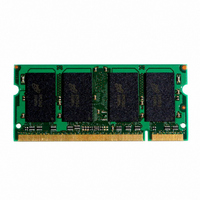
MT4HTF3264HY-667D3 Micron Technology Inc, MT4HTF3264HY-667D3 Datasheet - Page 13

MT4HTF3264HY-667D3
Manufacturer Part Number
MT4HTF3264HY-667D3
Description
MODULE DDR2 256MB 200SODIMM
Manufacturer
Micron Technology Inc
Datasheet
1.MT4HTF3264HY-667D3.pdf
(17 pages)
Specifications of MT4HTF3264HY-667D3
Memory Type
DDR2 SDRAM
Memory Size
256MB
Package / Case
200-SODIMM
Main Category
DRAM Module
Sub-category
DDR2 SDRAM
Module Type
200SODIMM
Device Core Size
64b
Organization
32Mx64
Total Density
256MByte
Chip Density
512Mb
Maximum Clock Rate
667MHz
Operating Supply Voltage (typ)
1.8V
Operating Current
1A
Number Of Elements
4
Operating Supply Voltage (max)
1.9V
Operating Supply Voltage (min)
1.7V
Operating Temp Range
0C to 70C
Operating Temperature Classification
Commercial
Pin Count
200
Mounting
Socket
Lead Free Status / RoHS Status
Lead free / RoHS Compliant
Speed
-
Lead Free Status / Rohs Status
Compliant
Other names
557-1304
MT4HTF3264HY-667D3
MT4HTF3264HY-667D3
Table 12: DDR2 I
Values shown for MT47H64M16 DDR2 SDRAM only and are computed from values specified in the 1Gb (64 Meg x 16) com-
ponent data sheet
PDF: 09005aef8161d160
htf4c16_32_64x64h.pdf - Rev. I 3/10 EN
Parameter
Operating one bank active-precharge current:
(I
Address bus inputs are switching; Data bus inputs are switching
Operating one bank active-read-precharge current: I
= CL (I
t
puts are switching; Data pattern is same as I
Precharge power-down current: All device banks idle;
LOW; Other control and address bus inputs are stable; Data bus inputs are float-
ing
Precharge quiet standby current: All device banks idle;
is HIGH, S# is HIGH; Other control and address bus inputs are stable; Data bus
inputs are floating
Precharge standby current: All device banks idle;
HIGH, S# is HIGH; Other control and address bus inputs are switching; Data bus
inputs are switching
Active power-down current: All device banks open;
t
stable; Data bus inputs are floating
Active standby current: All device banks open;
MAX (I
Other control and address bus inputs are switching; Data bus inputs are switching
Operating burst write current: All device banks open; Continuous burst
writes; BL = 4, CL = CL (I
t
are switching; Data bus inputs are switching
Operating burst read current: All device banks open; Continuous burst read,
I
t
inputs are switching; Data bus inputs are switching
Burst refresh current:
interval; CKE is HIGH, S# is HIGH between valid commands; Other control and
address bus inputs are switching; Data bus inputs are switching
Self refresh current: CK and CK# at 0V; CKE ≤ 0.2V; Other control and ad-
dress bus inputs are floating; Data bus inputs are floating
Operating bank interleave read current: All device banks interleaving
reads; I
(I
HIGH between valid commands; Address bus inputs are stable during deselects;
Data bus inputs are switching
RCD (I
CK (I
RP (I
OUT
RP =
DD
DD
),
),
= 0mA; BL = 4, CL = CL (I
DD
DD
t
t
t
RAS =
DD
RP (I
RC =
DD
DD
OUT
); CKE is HIGH, S# is HIGH between valid commands; Address bus inputs
); CKE is LOW; Other control and address bus inputs are
), AL = 0;
); CKE is HIGH, S# is HIGH between valid commands; Address bus in-
),
DD
= 0mA; BL = 4, CL = CL (I
t
t
RP =
RC (I
t
); CKE is HIGH, S# is HIGH between valid commands; Address bus
RAS MIN (I
DD
t
RP (I
t
CK =
),
DD
t
RRD =
DD
Specifications and Conditions – 512MB (Die Revision A)
DD
DD
t
t
); CKE is HIGH, S# is HIGH between valid commands;
CK (I
CK =
), AL = 0;
); CKE is HIGH, S# is HIGH between valid commands;
t
RRD (I
DD
DD
t
CK (I
), AL = 0;
),
t
RC =
DD
DD
DD
t
CK =
),
); REFRESH command at every
), AL =
t
t
RCD =
RC (I
t
128MB, 256MB, 512MB (x64, SR) 200-Pin DDR2 SODIMM
CK =
t
CK (I
DD4W
DD
t
RCD (I
t
t
),
DD
RCD (I
CK (I
t
),
RAS =
t
CK =
t
t
DD
RAS =
CK =
DD
t
DD
CK =
) - 1 ×
),
t
); CKE is HIGH, S# is
t
CK =
t
t
RAS MIN (I
CK (I
RAS =
t
CK (I
t
OUT
t
CK =
t
RAS MAX (I
t
CK (I
CK =
13
t
CK (I
DD
= 0mA; BL = 4, CL
DD
t
),
t
DD
RAS MAX (I
CK (I
),
Fast PDN exit
MR[12] = 0
Slow PDN exit
MR[12] = 1
t
t
DD
CK (I
); CKE is
RAS =
t
DD
RC =
);
t
RFC (I
DD
),
t
DD
DD
CK =
Micron Technology, Inc. reserves the right to change products or specifications without notice.
t
); CKE is
RCD =
t
t
),
); CKE
RC
RAS
DD
t
RP =
DD
t
CK
)
),
Symbol
I
I
I
I
I
I
I
DD4W
DD2Q
I
I
DD2N
DD3N
DD4R
I
I
I
DD2P
DD3P
DD0
DD1
DD5
DD6
DD7
-667
1080
1400
540
520
260
280
160
300
840
880
28
72
28
© 2005 Micron Technology, Inc. All rights reserved.
I
DD
-53E
1000
1360
440
480
180
200
140
240
720
720
28
72
28
Specifications
1320
-40E
440
460
160
160
140
220
640
640
960
28
72
28
Units
mA
mA
mA
mA
mA
mA
mA
mA
mA
mA
mA
mA


