PD3535 OSRAM Opto Semiconductors Inc, PD3535 Datasheet - Page 6
PD3535
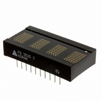
Manufacturer Part Number
PD3535
Description
DISPLAY PROGR 4CHAR 5X7 HE RED
Manufacturer
OSRAM Opto Semiconductors Inc
Datasheet
1.PD3535.pdf
(14 pages)
Specifications of PD3535
Size / Dimension
1.40" L x 0.72" W x 0.29" H (35.56mm x 18.29mm x 7.24mm)
Color
Red
Number Of Digits
4
Character Size
0.27 in
Illumination Color
High Efficiency Red
Wavelength
630 nm
Maximum Operating Temperature
+ 85 C
Minimum Operating Temperature
- 40 C
Luminous Intensity
90 ucd
Viewing Area (w X H)
6.86 mm x 5.08 mm
Display Type
5 x 7 Dot Matrix
Lead Free Status / RoHS Status
Lead free / RoHS Compliant
Configuration
-
Voltage - Forward (vf) Typ
-
Millicandela Rating
-
Internal Connection
-
Lead Free Status / Rohs Status
Details
Other names
475-1421
PD3535
Q68000A7964
PD3535
Q68000A7964
Available stocks
Company
Part Number
Manufacturer
Quantity
Price
Company:

Part Number:
PD3535
Manufacturer:
STANLEY
Quantity:
9 200


Timing Characteristics—Data “Write” Cycle
Notes:
1. Wait 1.0 µs between any Reads or Writes after writing a Control
2. All input voltages are V
Switching Specifications (V
2006-01-23
A0, A1
D0–D6
CE0, CE1
Write Cycle Timing
Para-
meter
T
T
T
T
T
T
T
T
T
T
T
T
RD
WR
Word with a Clear (D7=1). Wait 1.0 µs between any Reads or
Writes after Clearing a Control Word with a Clear (D7=0). All
other Reads and Writes can be back to back.
CLR
CLRD
AS
CES
RS
DS
W
AH
DH
CEH
RH
ACC
(1)
(1)
Description
Clear RAM
Clear RAM Disable
Address Setup
Chip Enable Setup
Read Enable Setup
Data Setup
Write Pulse
Address Hold
Data Hold
Chip Enable Hold
Read Enable Hold
Total Access
Time = Setup
Time + Write
Time + Hold Time
T CES
T AS
T RS
IL
=0.8 V, V
CC
=4.5 V)
Specification Minimum
–40°C
1.0
1.0
10
0
10
20
60
20
20
0
20
90
T W
T ACC
IH
T DS
=2.0 V.
25°C
1.0
1.0
10
0
10
30
70
30
30
0
30
110
T CEH
T AH
T DH
T RH
85°C
1.0
1.0
10
0
10
50
90
40
40
0
40
140
Units
µs
µs
ns
ns
ns
ns
ns
ns
ns
ns
ns
ns
2.0 V
0.8 V
2.0 V
0.8 V
2.0 V
0.8 V
2.0 V
0.8 V
2.0 V
0.8 V
*
*
*
*
*
6
Timing Characteristics—Data “Read” Cycle
3. These waveforms are not edge triggered.
4. Data out voltages are measured with 100 pF on the data bus
and the ability to source = –40 mA and sink=1.6 mA The rise and
fall times are 60 ns. V
Switching Specifications (V
A0–A3
D0–D6
WR
CE0, CE1
RD
Read Cycle Timing
Para-
meter
T
T
T
T
T
T
T
T
T
T
T
T
AS
CES
WS
DD
R
AH
DH
TRI
CEH
WH
ACC
WAIT
(1)
Description
Address Setup
Chip Enable
Write Enable Setup
Data Delay Time
Read Pulse
Address Hold
Data Hold
Time to Tristate
(Max. time)
Chip Enable Hold
Write Enable Hold
Total Access
Time = Setup
Time + Read
Time + Time to
Tristate
Wait Time between
Reads
T
T
T
PD243X, PD353X, PD443X
CES
AS
WS
OL
=0.4 V, V
CC
T
=4.5 V)
RACC
OH
Specification Minimum
–40°C
0
0
20
100
150
0
0
30
0
30
200
0
=2.4 V.
T
T
R
DATA OUT
DD
25°C
0
0
30
150
175
0
0
40
0
40
245
0
T
T
T
T
T
CEH
DH
AH
RI
WH
85°C
0
0
40
175
200
0
0
50
0
50
290
0
Units
ns
ns
ns
ns
ns
ns
ns
ns
ns
ns
ns
ns
2.0 V
0.8 V
2.0 V
0.8 V
2.0 V
0.8 V
2.0 V
0.8 V
2.0 V
0.8 V
*
*
*
*
*
Related parts for PD3535
Image
Part Number
Description
Manufacturer
Datasheet
Request
R

Part Number:
Description:
INTELLIGENT DISP 4CHAR 5X7 HERED
Manufacturer:
OSRAM Opto Semiconductors Inc
Datasheet:

Part Number:
Description:
DISPLAY 8DIGIT CERAMIC GREEN
Manufacturer:
OSRAM Opto Semiconductors Inc
Datasheet:

Part Number:
Description:
EMITTER IR 950NM 5MM SMD RADIAL
Manufacturer:
OSRAM Opto Semiconductors Inc
Datasheet:

Part Number:
Description:
LED TOPLED GREEN 570NM 2-PLCC
Manufacturer:
OSRAM Opto Semiconductors Inc
Datasheet:

Part Number:
Description:
INTERRUPTER RELFECT W/FILTR SMD
Manufacturer:
OSRAM Opto Semiconductors Inc
Datasheet:

Part Number:
Description:
LED Displays 5x7 Green 0.145 , 4-CHARACTER
Manufacturer:
OSRAM Opto Semiconductors Inc
Datasheet:

Part Number:
Description:
Q65110A4321_SIDELED PURE GREEN EOL150407
Manufacturer:
OSRAM Opto Semiconductors Inc
Datasheet:
Part Number:
Description:
Q65110A1202_RO DETECTOR 3/5MM_TR_RO
Manufacturer:
OSRAM Opto Semiconductors Inc
Datasheet:

Part Number:
Description:
PHOTODIODE 900NM 3MM W/FILTER
Manufacturer:
OSRAM Opto Semiconductors Inc
Datasheet:
Part Number:
Description:
INTELLIGENT DISP 4CHAR 5X7 HERED
Manufacturer:
OSRAM Opto Semiconductors Inc
Datasheet:
Part Number:
Description:
LED TOPLED GREEN 570NM 2-PLCC
Manufacturer:
OSRAM Opto Semiconductors Inc
Datasheet:
Part Number:
Description:
PHOTODIODE 900NM 3MM W/FILTER
Manufacturer:
OSRAM Opto Semiconductors Inc
Datasheet:

Part Number:
Description:
PHOTODIODE 850NM THRU-HOLE
Manufacturer:
OSRAM Opto Semiconductors Inc
Datasheet:

Part Number:
Description:
PHOTODIODE 880NM W/FILTER SMD
Manufacturer:
OSRAM Opto Semiconductors Inc
Datasheet: