PD3535 OSRAM Opto Semiconductors Inc, PD3535 Datasheet - Page 8
PD3535
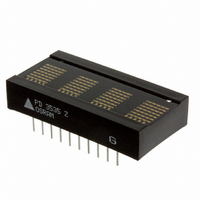
Manufacturer Part Number
PD3535
Description
DISPLAY PROGR 4CHAR 5X7 HE RED
Manufacturer
OSRAM Opto Semiconductors Inc
Datasheet
1.PD3535.pdf
(14 pages)
Specifications of PD3535
Size / Dimension
1.40" L x 0.72" W x 0.29" H (35.56mm x 18.29mm x 7.24mm)
Color
Red
Number Of Digits
4
Character Size
0.27 in
Illumination Color
High Efficiency Red
Wavelength
630 nm
Maximum Operating Temperature
+ 85 C
Minimum Operating Temperature
- 40 C
Luminous Intensity
90 ucd
Viewing Area (w X H)
6.86 mm x 5.08 mm
Display Type
5 x 7 Dot Matrix
Lead Free Status / RoHS Status
Lead free / RoHS Compliant
Configuration
-
Voltage - Forward (vf) Typ
-
Millicandela Rating
-
Internal Connection
-
Lead Free Status / Rohs Status
Details
Other names
475-1421
PD3535
Q68000A7964
PD3535
Q68000A7964
Available stocks
Company
Part Number
Manufacturer
Quantity
Price
Company:

Part Number:
PD3535
Manufacturer:
STANLEY
Quantity:
9 200


Functional Description
The block diagram includes 5 major blocks and internal registers
(indicated by dotted lines).
Display Memory consists of a 5 x 8 bit RAM block. Each of the
four 8-bit words holds 7-bits of ASCII data (bits D0–D6) and an
attribute select bit (Bit D6). The fifth 8-bit memory word is used
as a control word register. A detailed description of the control
register and its functions can be found in the Control Word sec-
tion. Each 8-bit word is addressable and can be read from or writ-
ten to.
The Control Logic dictates all of the features of the display
device and is discussed in the Control Word section of this data
sheet.
The Character Generator converts the 7-bit ASCII data into the
proper dot pattern for the 128 characters shown in the character
set chart.
The Clock Source can originate either from the internal oscillator
clock or from an external source—usually from the output of
another display in a multiple module array.
The Display Multiplexer controls all display output to the digit
drivers so no additional logic is required for a display system.
The Column Drivers are connected directly to the display.
The Display has four digits. Each of the four digits is com-prised of
35 LEDs in a 5 x 7 dot array which makes up the alphanumeric
characters.
The intensity of the display can be varied by the Control Word in
steps of 0% (Blank), 25%, 50%, and full brightness.
The Reset pin when activated clears the internal counter. A reset is
usually done after power up and is of very short duration-nanosec-
onds or microseconds. If the reset pin is held low for a longer time
(milliseconds) some or all LEDs in the bottom row may light up. The
appearance of lit LEDs during a “reset” is not an indication of a mal-
functioning part. It is advisable to keep the reset pulse as short as
possible to avoid displaying a row of lit LEDs.
Microprocessor Interface
The interface to the microprocessor is through the address lines.
(A0–A2), the data bus (D0–D7), two chip select lines (CE0, CE1),
and read (RD) and write (WR) lines.
The CE0 should be held low when executing a read, or write oper-
ation. CE1 must be held high.
The read and write lines are both active low. During a valid read
the data input lines (D0–D7) become outputs. A valid write will
enable the data as input lines.
Data Input Commands
2006-01-23
CEO
1
0
0
0
0
0
0
CE1
0
1
1
1
1
1
1
RD
X
0
1
1
1
1
1
WR
X
1
0
0
0
0
0
A2
X
1
1
1
1
1
1
A1
X
0
0
0
1
1
0
A0
X
0
0
1
0
1
0
D7
X
X
0
0
0
0
1
D6
X
X
0
1
1
0
X
D5
X
X
1
0
1
1
X
8
D4
X
X
0
1
0
1
X
Input Buffering
If a cable length of 6 inches or more is used, all inputs to the display
should be buffered with a tri-state non-inverting buffer mounted as
close to the display as conveniently possible. Recommended
buffers are: 74LS245 for the data lines and 74LS244 for the control
lines.
Block Diagram
Mode Selection
D0-D7
CE0, CE1
A0-A2
RD, WR
CLK SEL
XCLK
RST
CEO
0
1
X
X
0=Low logic level, 1=High logic level, X=Don’t care
D3
X
X
0
0
0
0
X
CE1
1
X
0
X
8
7
3
D2
X
X
1
1
1
0
X
Display Memory
Decode
Logic
OSC
RD
0
X
X
1
Mux
(RAM) 4 x 8
and
PD243X, PD353X, PD443X
D1
X
X
0
1
1
1
X
4
WR
0
X
X
1
D0
X
X
0
1
0
1
X
Display
3
5
Control
1 x 8
Reg
Operation
No Change
Read Digit 0 Data to Bus
($) Written to Digit 0
(W) Written to Digit 1
(f) Written to Digit 2
(3) Written to Digit 3
Char. Written to Digit 0 and
Cursor Enabled
Operation
None
None
None
None
Multiplexer
Display
Control
Output
Logic
14
8
1
20
1
128 Char
128 x 5
ROM
3
Column
Drivers
Drivers
Output
Latch
Row
IDBD5065
15
20
Related parts for PD3535
Image
Part Number
Description
Manufacturer
Datasheet
Request
R

Part Number:
Description:
INTELLIGENT DISP 4CHAR 5X7 HERED
Manufacturer:
OSRAM Opto Semiconductors Inc
Datasheet:

Part Number:
Description:
DISPLAY 8DIGIT CERAMIC GREEN
Manufacturer:
OSRAM Opto Semiconductors Inc
Datasheet:

Part Number:
Description:
EMITTER IR 950NM 5MM SMD RADIAL
Manufacturer:
OSRAM Opto Semiconductors Inc
Datasheet:

Part Number:
Description:
LED TOPLED GREEN 570NM 2-PLCC
Manufacturer:
OSRAM Opto Semiconductors Inc
Datasheet:

Part Number:
Description:
INTERRUPTER RELFECT W/FILTR SMD
Manufacturer:
OSRAM Opto Semiconductors Inc
Datasheet:

Part Number:
Description:
LED Displays 5x7 Green 0.145 , 4-CHARACTER
Manufacturer:
OSRAM Opto Semiconductors Inc
Datasheet:

Part Number:
Description:
Q65110A4321_SIDELED PURE GREEN EOL150407
Manufacturer:
OSRAM Opto Semiconductors Inc
Datasheet:
Part Number:
Description:
Q65110A1202_RO DETECTOR 3/5MM_TR_RO
Manufacturer:
OSRAM Opto Semiconductors Inc
Datasheet:

Part Number:
Description:
PHOTODIODE 900NM 3MM W/FILTER
Manufacturer:
OSRAM Opto Semiconductors Inc
Datasheet:
Part Number:
Description:
INTELLIGENT DISP 4CHAR 5X7 HERED
Manufacturer:
OSRAM Opto Semiconductors Inc
Datasheet:
Part Number:
Description:
LED TOPLED GREEN 570NM 2-PLCC
Manufacturer:
OSRAM Opto Semiconductors Inc
Datasheet:
Part Number:
Description:
PHOTODIODE 900NM 3MM W/FILTER
Manufacturer:
OSRAM Opto Semiconductors Inc
Datasheet:

Part Number:
Description:
PHOTODIODE 850NM THRU-HOLE
Manufacturer:
OSRAM Opto Semiconductors Inc
Datasheet:

Part Number:
Description:
PHOTODIODE 880NM W/FILTER SMD
Manufacturer:
OSRAM Opto Semiconductors Inc
Datasheet: