CU40025-UW6J Noritake Company Inc, CU40025-UW6J Datasheet - Page 10
CU40025-UW6J
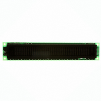
Manufacturer Part Number
CU40025-UW6J
Description
MODULE VF DISPLAY 40X2 5MM CHAR
Manufacturer
Noritake Company Inc
Series
U-Versionr
Specifications of CU40025-UW6J
Outline L X W X H
182.00mm x 33.50mm x 20.50mm
Viewing Area
138.80mm L x 11.50mm W
Display Format
40 x 2
Display Type
Character
Format
5 x 7 Dots
Voltage - Supply
5V
Character Size
4.70mm H x 2.30mm W
Operating Temperature
-40°C ~ 85°C
Resolution
2 X 40
Viewing Area (h X W)
11.5mm X 138.8mm
Supply Current
300mA
Supply Voltage Range
4.75V To 5.25V
Character Format
Dot Matrix
Character Type
5x7 Dot Matrix
External Depth
21mm
External
RoHS Compliant
Product
Character Display Modules
Character Count X Line
40 x 2
Module Size (w X H X T)
182 mm x 33.5 mm x 20.5 mm
Voltage Rating
5 V
Operating Temperature Range
- 40 C to + 85 C
Current Rating
300 mA
Dot Format
5 x 7
Viewing Area (w X H)
138.8 mm x 11.5 mm
Interface
Parallel / Serial
Lead Free Status / RoHS Status
Lead free / RoHS Compliant
Number Of Dots
-
Lead Free Status / Rohs Status
Details
Other names
286-1062
Available stocks
Company
Part Number
Manufacturer
Quantity
Price
Company:

Part Number:
CU40025-UW6J
Manufacturer:
Noritake Company Inc
Quantity:
135


7.10. Write Data
7.11. Read Data
7.12. Read Busy Flag/Address Counter
RS = 1
This instruction writes the data in DB7 to DB0 into either the CG RAM or the DD RAM.
The RAM space (CG or DD), and the address in that space, that is accessed depends on
whether a “Set CG RAM Address” or “Set DD RAM Address” instruction was last executed,
and on the parameters of that instruction. The contents of the address counter will be
automatically modified after each “Write Data”, as determined by the “7.4 Entry Mode Set”.
When data is written to the CG RAM, the DB7, DB6 and DB5 bits are not displayed as
characters.
RS = 1
This instruction reads data from either CG RAM or DD RAM, depending on the type of “Set
RAM Address” instructions last sent. The address in that space depends on the “Set RAM
Address” instruction parameters. Immediately before executing “Read Data”, “Set CG RAM
Address” or “Set DD RAM Address” must be executed. The contents of the address counter
are modified after each “Read Data”, as determined by the “7.4 Entry Mode Set”. Display shift
is not executed, as described at of the “7.4 Entry Mode Set”.
RS = 0
Reading the instruction register yields the current value of the address counter and the busy
flag. This instruction must be executed prior to any other instructions. ACC, the address
counter value, will point to a location in either CG RAM or DD RAM, depending on the type
of “Set RAM Address” instruction last sent.
In “Busy Flag Check” immediately after executing “Write Data” instruction, a valid address
counter value can be ready as soon as BF goes low. The BF bit shows the status of the busy
flag.
DB7 DB6 DB5 DB4 DB3 DB2 DB1 DB0
DB7
DB7
BF
BF = 1 : busy.
BF = 0 : ready for next instruction, command receivable.
DB6
DB6
DB5
DB5
DATA WRITE
DATA READ
DB4
DB4
ACC
DB3
DB3
DB2
DB2
9
DB1
DB1
DB0
DB0
00H to FFH
CU40025-UW6J
Related parts for CU40025-UW6J
Image
Part Number
Description
Manufacturer
Datasheet
Request
R


Part Number:
Description:
MODULE VF GRAPHIC DISPLAY 112X16
Manufacturer:
Noritake Company Inc
Datasheet:

Part Number:
Description:
MODULE VF DISPLY 16X2 4.8MM CHAR
Manufacturer:
Noritake Company Inc
Datasheet:

Part Number:
Description:
MODULE VF GRAPHIC DISPLAY 140X16
Manufacturer:
Noritake Company Inc
Datasheet:

Part Number:
Description:
MODULE VF DISPLAY 20X2 EXT TEMP
Manufacturer:
Noritake Company Inc
Datasheet:

Part Number:
Description:
MODULE VF DISPLAY 24X2 5MM CHAR
Manufacturer:
Noritake Company Inc
Datasheet:

Part Number:
Description:
MODULE VF GRAPHIC DISPLAY 140X32
Manufacturer:
Noritake Company Inc
Datasheet:

Part Number:
Description:
MODULE VF DISPLAY 24X4 5V CHAR
Manufacturer:
Noritake Company Inc
Datasheet:

Part Number:
Description:
MODULE VF DISPLAY 20X2 5V CHAR
Manufacturer:
Noritake Company Inc
Datasheet:

Part Number:
Description:
MODULE VF DISPLAY 20X2 5V CHAR
Manufacturer:
Noritake Company Inc
Datasheet:

Part Number:
Description:
MODULE VF DISPLAY 24X4 5V CHAR
Manufacturer:
Noritake Company Inc
Datasheet:

Part Number:
Description:
MODULE VF DISP 16X2 8MM CHAR
Manufacturer:
Noritake Company Inc
Datasheet:

Part Number:
Description:
MODULE VF GRAPHIC DISPLAY 140X16
Manufacturer:
Noritake Company Inc
Datasheet:

Part Number:
Description:
MODULE VF DISPLAY 24X6 5V CHAR
Manufacturer:
Noritake Company Inc
Datasheet:

Part Number:
Description:
MODULE VF DISPLAY 24X6 5V CHAR
Manufacturer:
Noritake Company Inc
Datasheet: