HFBR-2115TZ Avago Technologies US Inc., HFBR-2115TZ Datasheet - Page 4
HFBR-2115TZ
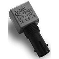
Manufacturer Part Number
HFBR-2115TZ
Description
RCVR MODULE 1300NM 125M 16DIP ST
Manufacturer
Avago Technologies US Inc.
Datasheet
1.HFBR-2115TZ.pdf
(12 pages)
Specifications of HFBR-2115TZ
Data Rate
125MBd
Voltage - Supply
4.5 V ~ 5.5 V
Power - Minimum Receivable
-34.5dBm
Current - Supply
82mA
Applications
General Purpose
Data Rate Max
0.1Gbps
Wavelength Typ
1300nm
Peak Reflow Compatible (260 C)
Yes
Leaded Process Compatible
Yes
Connector Type
Plastic ST
Lead Free Status / RoHS Status
Lead free / RoHS Compliant


These parameters are reflected in
the guaranteed performance of the
transmitter and receiver specifica-
tions in this data sheet. This same
model has been used extensively in
the ANSI and IEEE committees,
including the ANSI X3T9.5
committee, to establish the optical
performance requirements for
various fiber-optic interface
standards. The cable parameters
used come from the ISO/IEC JTC1/
SC 25/WG3 Generic Cabling for
Customer Premises per DIS 11801
document and the EIA/TIA-568-A
Commercial Building Telecom-
munications Cabling Standard per
SP-2840.
Transmitter and Receiver Signaling
Rate Range and BER Performance
For purposes of definition, the
symbol rate (Baud), also called
signaling rate, is the reciprocal of
the symbol time. Data rate (bits/
sec) is the symbol rate divided by
the encoding factor used to encode
the data (symbols/bit).
When used in FDDI, ATM 100
Mbps, and Fast Ethernet
applications, the performance of
Avago’s 1300 nm HFBR-1115/-
2115 data link modules is
guaranteed over the signaling rate
of 10 MBd to 125 MBd to the full
conditions listed in the individual
product specification tables.
The data link modules can be used
for other applications at signaling
rates outside of the 10 MBd to 125
MBd range with some penalty in
the link optical power budget
primarily caused by a reduction of
receiver sensitivity. Figure 5 gives
an indication of the typical
performance of these 1300 nm
products at different rates.
4
2.5 x 10
Figure 5. Transmitter/Receiver relative optical
power budget at constant BER vs. signaling
rate.
These data link modules can also
be used for applications which
require different bit-error-ratio
(BER) performance. Figure 6
illustrates the typical trade-off
between link BER and the receiver
input optical power level.
Figure 6. Bit-error-ratio vs. relative receiver
input optical power.
CONDITIONS:
1. PRBS 2
2. DATA SAMPLED AT CENTER OF DATA SYMBOL.
3. BER = 10
4. T
5. V
6. INPUT OPTICAL RISE/FALL TIMES = 1.0/2.1 ns.
1 x 10
1 x 10
1 x 10
1 x 10
1 x 10
1 x 10
1 x 10
1 x 10
1 x 10
A
CC
CONDITIONS:
1. 125 MBd
2. PRBS 2
3. T
4. V
5. INPUT OPTICAL RISE/FALL TIMES = 1.0/2.1 ns.
3.0
2.5
2.0
1.5
1.0
0.5
= 25° C
-10
-11
-12
-2
-3
-4
-5
-6
-7
-8
= 5 Vdc
RELATIVE INPUT OPTICAL POWER – dB
0
A
CC
-6
0
= 25° C
7
= 5 Vdc
-1
-6
25
7
-1
-4
50
SIGNAL RATE (MBd)
CENTER OF
SYMBOL
-2
75 100 125
0
2
150
175
4
200
Data Link Jitter Performance
The Avago 1300 nm data link
modules are designed to operate
per the system jitter allocations
stated in Table E1 of Annex E of
the FDDI PMD standard.
The 1300 nm transmitter will
tolerate the worst-case input
electrical jitter allowed in the table
without violating the worst-case
output jitter requirements of
Section 8.1 Active Output Interface
of the FDDI PMD standard.
The 1300 nm receiver will tolerate
the worst-case input optical jitter
allowed in Section 8.2 Active Input
Interface of the FDDI PMD
standard without violating the
worst-case output electrical jitter
allowed in the Table E1 of the
Annex E.
The jitter specifications stated in
the following transmitter and
receiver specification table are
derived from the values in Table
E1 of Annex E. They represent the
worst-case jitter contribution that
the transmitter and receiver are
allowed to make to the overall
system jitter without violating the
Annex E allocation example. In
practice, the typical jitter
contribution of the Avago data link
modules is well below the
maximum amounts.
Recommended Handling Precautions
It is advised that normal static
precautions be taken in the
handling and assembly of these
data link modules to prevent
damage which may be induced by
electrostatic discharge (ESD). The
HFBR-1115/-2115 series meets
MIL-STD-883C Method 3015.4
Class 2.
Care should be taken to avoid
shorting the receiver Data or
Signal Detect Outputs directly to
ground without proper current-
limiting impedance.
Related parts for HFBR-2115TZ
Image
Part Number
Description
Manufacturer
Datasheet
Request
R

Part Number:
Description:
FIBER OPTIC CONN LATCH GRY SIMPL
Manufacturer:
Avago Technologies US Inc.
Datasheet:

Part Number:
Description:
FIBER OPTIC CONN LATCH BLU SIMPL
Manufacturer:
Avago Technologies US Inc.
Datasheet:

Part Number:
Description:
FIBER OPTIC CRIMPLESS CONN GRAY
Manufacturer:
Avago Technologies US Inc.
Datasheet:

Part Number:
Description:
FIBER OPTIC CONN BLUE SIMPLEX
Manufacturer:
Avago Technologies US Inc.
Datasheet:

Part Number:
Description:
FIBER OPTIC CONN LATCH DUPLEX
Manufacturer:
Avago Technologies US Inc.
Datasheet:

Part Number:
Description:
FIBER OPTIC CONN DUPLEX
Manufacturer:
Avago Technologies US Inc.
Datasheet:

Part Number:
Description:
FIBER OPTIC CONN GRAY SIMPLEX
Manufacturer:
Avago Technologies US Inc.
Datasheet:

Part Number:
Description:
FIBER OPTIC CBL DUPLEX 1=100M
Manufacturer:
Avago Technologies US Inc.
Datasheet:

Part Number:
Description:
FIBER OPTIC CBL DUPLEX 1=500M
Manufacturer:
Avago Technologies US Inc.
Datasheet:

Part Number:
Description:
FIBER OPTIC CBL CONN DUPLEX 5M
Manufacturer:
Avago Technologies US Inc.
Datasheet:

Part Number:
Description:
OPTOCOUPLER GATE DRV 2A 16-SOIC
Manufacturer:
Avago Technologies US Inc.
Datasheet:
Part Number:
Description:
OPTOCOUPLER 2CH 2.5A 16-SOIC
Manufacturer:
Avago Technologies US Inc.
Datasheet:

Part Number:
Description:
OPTOCOUPLER GATE DRV 0.4A 16SOIC
Manufacturer:
Avago Technologies US Inc.
Datasheet:

Part Number:
Description:
OPTOCOUPLER 2.0A 250KHZ 8-DIP
Manufacturer:
Avago Technologies US Inc.
Datasheet:

Part Number:
Description:
OPTOCOUPLER 2.0A 250KHZ GW 8-SMD
Manufacturer:
Avago Technologies US Inc.
Datasheet: