AFBR-5803AZ Avago Technologies US Inc., AFBR-5803AZ Datasheet - Page 15
AFBR-5803AZ
Manufacturer Part Number
AFBR-5803AZ
Description
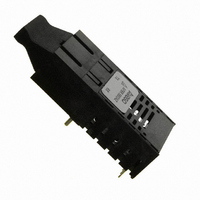
TXRX OPT 1X9 100MBPS SC EXT TEMP
Manufacturer
Avago Technologies US Inc.
Datasheet
1.AFBR-5803ATZ.pdf
(16 pages)
Specifications of AFBR-5803AZ
Data Rate
100Mbps
Wavelength
1300nm
Applications
General Purpose
Voltage - Supply
3.3V, 5V
Connector Type
SC
Mounting Type
Through Hole
Function
Implement FDDI and ATM at the 100 Mbps/125 MBd rate
Product
Transceiver
Pulse Width Distortion
0.69 ns (Max)/2.14 ns (Max)
Maximum Output Current
50 mA
Operating Supply Voltage
4.75 V to 5.25 V
Maximum Operating Temperature
+ 85 C
Minimum Operating Temperature
- 10 C
Lead Free Status / RoHS Status
Lead free / RoHS Compliant
For Use With
Multimode Glass
Lead Free Status / RoHS Status
Lead free / RoHS Compliant, Lead free / RoHS Compliant
Other names
516-1989
Available stocks
Company
Part Number
Manufacturer
Quantity
Price
Company:

Part Number:
AFBR-5803AZ
Manufacturer:
Avago Technologies US Inc.
Quantity:
135
Company:
Part Number:
AFBR-5803AZ
Manufacturer:
AVAGO
Quantity:
100
Part Number:
AFBR-5803AZ
Manufacturer:
AVAGO/安华高
Quantity:
20 000


13. The transmitter provides compliance with the need for Transmit_Disable commands from the FDDI SMT layer by providing an Output Optical
14. This parameter complies with the FDDI PMD requirements for the trade-offs between center wavelength, spectral width, and rise/fall times
15. This parameter complies with the optical pulse envelope from the FDDI PMD shown in Figure 10. The optical rise and fall times are measured
16. Duty Cycle Distortion contributed by the transmitter is measured at a 50% threshold using an IDLE Line State, 125 MBd
17. Data Dependent Jitter contributed by the transmitter is specified with the FDDI test pattern described in FDDI PMD Annex A.5. See Application
18. Random Jitter contributed by the transmitter is specified with an IDLE Line State, 125 MBd (62.5 MHz square-wave), input signal. See Application
19. This specification is intended to indicate the performance of the receiver section of the transceiver when Input Optical Power signal character-
20. All conditions of Note 19 apply except that the measurement is made at the center of the symbol with no window time-width.
21. This value is measured during the transition from low to high levels of input optical power.
22. The Signal Detect output shall be asserted within 100 µs after a step increase of the Input Optical Power. The step will be from a low Input
23. This value is measured during the transition from high to low levels of input optical power. The maximum value will occur when the input optical
24. Signal detect output shall be de-asserted within 350 µs after a step decrease in the Input Optical Power from a level which is the lower of; -31
Power level of < -45 dBm average in response to a logic “0” input. This specification applies to either 62.5/125 µm or 50/125 µm fiber cables.
shown in Figure 9.
from 10% to 90% when the transmitter is driven by the FDDI HALT Line State (12.5 MHz square-wave) input signal.
(62.5 MHz square-wave), input signal. See Application Information - Transceiver Jitter Performance Section of this data sheet for further de-
tails.
Information - Transceiver Jitter Performance Section of this data sheet for further details.
Information - Transceiver Jitter Performance Section of this data sheet for further details.
istics are present per the following definitions. The Input Optical Power dynamic range from the minimum level (with a window time-width) to
the maximum level is the range over which the receiver is guaranteed to provide output data with a Bit Error Ratio (BER) better than or equal
to 2.5 x 10
• At the Beginning of Life (BOL)
• Over the specified operating temperature and voltage ranges
• Input symbol pattern is the FDDI test pattern defined in FDDI PMD Annex A.5 with 4B/5B NRZI encoded data that contains a duty cycle base-
• Receiver data window time-width is 2.13 ns or greater and centered at mid-symbol. This worst case window time-width is the minimum al-
To test a receiver with the worst case FDDI PMD Active Input jitter condition requires exacting control over DCD, DDJ and RJ jitter components
that is difficult to implement with production test equipment. The receiver can be equivalently tested to the worst case FDDI PMD input jitter
conditions and meet the minimum output data window time-width of 2.13 ns. This is accomplished by using a nearly ideal input optical signal
(no DCD, insignificant DDJ and RJ) and measuring for a wider window time-width of 4.6 ns. This is possible due to the cumulative effect of
jitter components through their superposition (DCD and DDJ are directly additive and RJ components are rms additive). Specifically, when a
nearly ideal input optical test signal is used and the maximum receiver peak-to-peak jitter contributions of DCD (0.4 ns), DDJ (1.0 ns), and RJ
(2.14 ns) exist, the minimum window time-width becomes 8.0 ns -0.4 ns - 1.0 ns - 2.14 ns = 4.46 ns, or conservatively 4.6 ns. This wider window
time-width of 4.6 ns guarantees the FDDI PMD Annex E minimum window time-width of 2.13 ns under worst case input jitter conditions to the
Avago Technologies receiver.
• Transmitter operating with an IDLE Line State pattern, 125 MBd (62.5 MHz square-wave), input signal to simulate any cross-talk present
Optical Power, -45 dBm, into the range between greater than P
time, LS_Max (15 µs) after Signal Detect has been asserted. See Figure 12 for more information.
power is either -45 dBm average or when the input optical power yields a BER of 10
dBm or P
have occurred in less than 8 ns. The receiver output will have a BER of 10
The input data stream is the Quiet Line State. Also, signal detect will be de-asserted within a maximum of 350 µs after the BER of the receiver
output degrades above 10
12 for more information.
line wander effect of 50 kHz. This sequence causes a near worst case condition for inter-symbol interference.
lowed eye-opening presented to the FDDI PHY PM._Data indication input (PHY input) per the example in FDDI PMD Annex E. This minimum
window time-width of 2.13 ns is based upon the worst case FDDI PMD Active Input Interface optical conditions for peak-to-peak DCD (1.0
ns), DDJ (1.2 ns) and RJ (0.76 ns) presented to the receiver.
between the transmitter and receiver sections of the transceiver.
D
-10
+ 4 dB (P
.
D
is the power level at which signal detect was de-asserted), to a power level of -45 dBm or less. This step decrease will
-2
for an input optical data stream that decays with a negative ramp function instead of a step function. See Figure
A
, and -14 dBm. The BER of the receiver output will be 10
-2
or better for a period of 12 µs or until signal detect is de-asserted.
-2
or larger, whichever power is higher.
-2
or better during the
Related parts for AFBR-5803AZ
Image
Part Number
Description
Manufacturer
Datasheet
Request
R

Part Number:
Description:
650nm FE Transceiver Eval Kit
Manufacturer:
Avago Technologies US Inc.
Datasheet:

Part Number:
Description:
TXRX OPT OC3 MTRJ SFF 2X5DIP
Manufacturer:
Avago Technologies US Inc.
Datasheet:

Part Number:
Description:
TXRX ETHERNET 125MBD MMF 2X5
Manufacturer:
Avago Technologies US Inc.
Datasheet:

Part Number:
Description:
TXRX OPT SFP DGTL 850NM IND
Manufacturer:
Avago Technologies US Inc.
Datasheet:

Part Number:
Description:
TXRX OPT SFF 4/2/1GBD 2X7
Manufacturer:
Avago Technologies US Inc.
Datasheet:

Part Number:
Description:
TXRX OPT SFP 4/2/1GBD 850NM
Manufacturer:
Avago Technologies US Inc.
Datasheet:

Part Number:
Description:
TXRX OPT XFP 10GB/S 850NM
Manufacturer:
Avago Technologies US Inc.
Datasheet:

Part Number:
Description:
TXRX OPT 1X9 100MBPS ST EXT TEMP
Manufacturer:
Avago Technologies US Inc.
Datasheet:

Part Number:
Description:
TXRX OPT 1X9 100MBPS DUPLEX SC
Manufacturer:
Avago Technologies US Inc.
Datasheet:

Part Number:
Description:
TXRX OPT 1X9 100MBPS DUPLEX ST
Manufacturer:
Avago Technologies US Inc.
Datasheet:

Part Number:
Description:
OPTOCOUPLER GATE DRV 2A 16-SOIC
Manufacturer:
Avago Technologies US Inc.
Datasheet:
Part Number:
Description:
OPTOCOUPLER 2CH 2.5A 16-SOIC
Manufacturer:
Avago Technologies US Inc.
Datasheet:

Part Number:
Description:
OPTOCOUPLER GATE DRV 0.4A 16SOIC
Manufacturer:
Avago Technologies US Inc.
Datasheet:

Part Number:
Description:
OPTOCOUPLER 2.0A 250KHZ 8-DIP
Manufacturer:
Avago Technologies US Inc.
Datasheet:

Part Number:
Description:
OPTOCOUPLER 2.0A 250KHZ GW 8-SMD
Manufacturer:
Avago Technologies US Inc.
Datasheet: