AFBR-5803AZ Avago Technologies US Inc., AFBR-5803AZ Datasheet - Page 6
AFBR-5803AZ
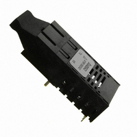
Manufacturer Part Number
AFBR-5803AZ
Description
TXRX OPT 1X9 100MBPS SC EXT TEMP
Manufacturer
Avago Technologies US Inc.
Datasheet
1.AFBR-5803ATZ.pdf
(16 pages)
Specifications of AFBR-5803AZ
Data Rate
100Mbps
Wavelength
1300nm
Applications
General Purpose
Voltage - Supply
3.3V, 5V
Connector Type
SC
Mounting Type
Through Hole
Function
Implement FDDI and ATM at the 100 Mbps/125 MBd rate
Product
Transceiver
Pulse Width Distortion
0.69 ns (Max)/2.14 ns (Max)
Maximum Output Current
50 mA
Operating Supply Voltage
4.75 V to 5.25 V
Maximum Operating Temperature
+ 85 C
Minimum Operating Temperature
- 10 C
Lead Free Status / RoHS Status
Lead free / RoHS Compliant
For Use With
Multimode Glass
Lead Free Status / RoHS Status
Lead free / RoHS Compliant, Lead free / RoHS Compliant
Other names
516-1989
Available stocks
Company
Part Number
Manufacturer
Quantity
Price
Company:

Part Number:
AFBR-5803AZ
Manufacturer:
Avago Technologies US Inc.
Quantity:
135
Company:
Part Number:
AFBR-5803AZ
Manufacturer:
AVAGO
Quantity:
100
Part Number:
AFBR-5803AZ
Manufacturer:
AVAGO/安华高
Quantity:
20 000


Figure 6. Bit Error Rate vs. Relative Receiver Input Optical Power.
NOTES:
THE SPLIT-LOAD TERMINATIONS FOR ECL SIGNALS NEED TO BE LOCATED AT THE INPUT
R1 = R4 = R6 = R8 = R10 = 130 OHMS FOR +5.0 V OPERATION, 82 OHMS FOR +3.3 V OPERATION.
R2 = R3 = R5 = R7 = R9 = 82 OHMS FOR +5.0 V OPERATION, 130 OHMS FOR +3.3 V OPERATION.
C1 = C2 = C3 = C5 = C6 = 0.1 µF.
C4 = 10 µF.
L1 = L2 = 1 µH COIL OR FERRITE INDUCTOR.
Figure 7. Recommended Decoupling and Termination Circuits
TERMINATION
AT PHY
DEVICE
INPUTS
OF DEVICES RECEIVING THOSE ECL SIGNALS. RECOMMEND 4-LAYER PRINTED CIRCUIT
BOARD WITH 50 OHM MICROSTRIP SIGNAL PATHS BE USED.
1 x 10
1 x 10
1 x 10
1 x 10
1 x 10
1 x 10
1 x 10
1 x 10
1 x 10
1 x 10
1 x 10
CONDITIONS:
1. 155 MBd
2. PRBS 2
3. CENTER OF SYMBOL SAMPLING
4. T
5. V
6. INPUT OPTICAL RISE/FALL TIMES = 1.0/2.1 ns.
-10
-11
-12
-2
-3
-4
-5
-6
-7
-8
-9
A
CC
NO INTERNAL CONNECTION
-6
= +25˚C
= 3.3 V to 5 V dc
V
Rx
R6
RELATIVE INPUT OPTICAL POWER - dB
EE
1
7
-1
RD
-4
R5
RD
2
V
CC
C6
RD
R7
RD
-2
3
R8
AFBR-5803 SERIES
Rx
CENTER OF SYMBOL
SD
SD
4
0
AFBR-5803Z
TOP VIEW
R10
R9
C1
TRANSCEIVER
V
AT V
C3
Rx
V
CC
5
CC
L1
V
FILTER
CC
2
CC
PINS
NO INTERNAL CONNECTION
V
Tx
CC
6
C4
L2
Tx
C2
4
TD
7
TD
TERMINATION
AT TRANSCEIVER
INPUTS
R1
TD
R2
8
V
CC
V
Tx
C5
EE
R3
9
R4
TD
Transceiver Jitter Performance
TheAvago Technologies 1300 nm transceivers are
designed to operate per the system jitter allocations
stated in Tables E1 of Annexes E of the FDDI PMD and
LCF-PMD standards.
The Avago Technologies1300 nm transmitters will
tolerate the worst case input electrical jitter allowed in
these tables without violating the worst case output jitter
requirements of Sections 8.1 Active Output Interface of
the FDDI PMD and LCF-PMD standards.
The Avago Technologies 1300 nm receivers will tolerate
the worst case input optical jitter allowed in Sections 8.2
Active Input Interface of the FDDI PMD and LCF-PMD
standards without violating the worst case output electri-
cal jitter allowed in the Tables E1 of the Annexes E.
The jitter specifications stated in the following 1300 nm
transceiver specification tables are derived from the
values in Tables E1 of Annexes E. They represent the worst
case jitter contribution that the transceivers are allowed
to make to the overall system jitter without violating the
Annex E allocation example. In practice the typical con-
tribution of the Avago Technologies transceivers is well
below these maximum allowed amounts.
Recommended Handling Precautions
Avago Technologies recommends that normal static pre-
cautions be taken in the handling and assembly of these
transceivers to prevent damage which may be induced
by electrostatic discharge (ESD). The AFBR-5800 series of
transceivers meet MIL-STD-883C Method 3015.4 Class 2
products.
Care should be used to avoid shorting the receiver data
or signal detect outputs directly to ground without
proper current limiting impedance.
Related parts for AFBR-5803AZ
Image
Part Number
Description
Manufacturer
Datasheet
Request
R

Part Number:
Description:
650nm FE Transceiver Eval Kit
Manufacturer:
Avago Technologies US Inc.
Datasheet:

Part Number:
Description:
TXRX OPT OC3 MTRJ SFF 2X5DIP
Manufacturer:
Avago Technologies US Inc.
Datasheet:

Part Number:
Description:
TXRX ETHERNET 125MBD MMF 2X5
Manufacturer:
Avago Technologies US Inc.
Datasheet:

Part Number:
Description:
TXRX OPT SFP DGTL 850NM IND
Manufacturer:
Avago Technologies US Inc.
Datasheet:

Part Number:
Description:
TXRX OPT SFF 4/2/1GBD 2X7
Manufacturer:
Avago Technologies US Inc.
Datasheet:

Part Number:
Description:
TXRX OPT SFP 4/2/1GBD 850NM
Manufacturer:
Avago Technologies US Inc.
Datasheet:

Part Number:
Description:
TXRX OPT XFP 10GB/S 850NM
Manufacturer:
Avago Technologies US Inc.
Datasheet:

Part Number:
Description:
TXRX OPT 1X9 100MBPS ST EXT TEMP
Manufacturer:
Avago Technologies US Inc.
Datasheet:

Part Number:
Description:
TXRX OPT 1X9 100MBPS DUPLEX SC
Manufacturer:
Avago Technologies US Inc.
Datasheet:

Part Number:
Description:
TXRX OPT 1X9 100MBPS DUPLEX ST
Manufacturer:
Avago Technologies US Inc.
Datasheet:

Part Number:
Description:
OPTOCOUPLER GATE DRV 2A 16-SOIC
Manufacturer:
Avago Technologies US Inc.
Datasheet:
Part Number:
Description:
OPTOCOUPLER 2CH 2.5A 16-SOIC
Manufacturer:
Avago Technologies US Inc.
Datasheet:

Part Number:
Description:
OPTOCOUPLER GATE DRV 0.4A 16SOIC
Manufacturer:
Avago Technologies US Inc.
Datasheet:

Part Number:
Description:
OPTOCOUPLER 2.0A 250KHZ 8-DIP
Manufacturer:
Avago Technologies US Inc.
Datasheet:

Part Number:
Description:
OPTOCOUPLER 2.0A 250KHZ GW 8-SMD
Manufacturer:
Avago Technologies US Inc.
Datasheet: