AFBR-5930Z Avago Technologies US Inc., AFBR-5930Z Datasheet - Page 4
AFBR-5930Z
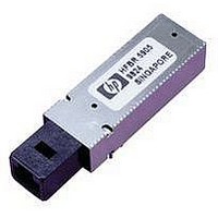
Manufacturer Part Number
AFBR-5930Z
Description
TXRX SBCON 200MBD 2X5 DIP
Manufacturer
Avago Technologies US Inc.
Datasheet
1.AFBR-5930Z.pdf
(14 pages)
Specifications of AFBR-5930Z
Applications
General Purpose
Data Rate
200MBd
Wavelength
1300nm
Voltage - Supply
3.135 V ~ 3.465 V
Connector Type
MTRJ
Mounting Type
Through Hole
Data Rate Max
0.2Gbps
Supply Voltage
3.3V
Wavelength Typ
1300nm
Leaded Process Compatible
Yes
Lead Free Status / RoHS Status
Lead free / RoHS Compliant


Pin Descriptions:
Pin 1 Receiver Signal Ground V
Directly connect this pin to the receiver ground plane.
Pin 2 Receiver Power Supply V
Provide +3.3 V dc via the recommended receiver power
supply filter circuit. Locate the power supply filter circuit as
close as possible to the V
Pin 3 Signal Detect SD:
Normal optical input levels to the receiver result in a logic
“1” output.
Low optical input levels to the receiver result in a fault
condition indicated by a logic “0” output.
This Signal Detect output can be used to drive a PECL
input on an upstream circuit, such as Signal Detect input
or Loss of Signal-bar.
Pin 4 Receiver Data Out Bar RD-:
No internal terminations are provided. See recommended
circuit schematic.
Pin 5 Receiver Data Out RD+:
No internal terminations are provided. See recommended
circuit schematic.
RECEIVER SIGNAL GROUND
RECEIVER POWER SUPPLY
RECEIVER DATA OUT BAR
RECEIVER DATA OUT
SIGNAL DETECT
Figure 3. Pin Out Diagram.
o
o
o
o
o
CC
RX
1
2
3
4
5
RX pin.
View
Top
EE
CC
TX
10
RX:
RX:
9
8
7
6
o
o
o
o
o
TRANSMITTER DATA IN BAR
TRANSMITTER DATA IN
TRANSMITTER DISABLE (LASER BASED PRODUCTS ONLY)
TRANSMITTER SIGNAL GROUND
TRANSMITTER POWER SUPPLY
Studs/Solder
Mounting
Posts
Pin 6 Transmitter Power Supply V
Provide +3.3 V dc via the recommended transmitter power
supply filter circuit. Locate the power supply filter circuit as
close as possible to the V
Pin 7 Transmitter Signal Ground V
Directly connect this pin to the transmitter ground plane.
Pin 8 Transmitter Disable T
No internal connection. Optional feature for laser based
products only. For laser based products connect this pin
to +3.3 V TTL logic high “1” to disable module. To enable
module connect to TTL logic low “0”.
Pin 9 Transmitter Data In TD+:
No internal terminations are provided. See recommended
circuit schematic.
Pin 10 Transmitter Data In Bar TD-:
No internal terminations are provided. See recommended
circuit schematic.
Mounting Studs/Solder Posts
The mounting studs are provided for transceiver mechani-
cal attachment to the circuit board. It is recommended
that the holes in the circuit board be connected to chassis
ground.
CC
DIS
TX pin.
:
CC
EE
TX:
TX:
Related parts for AFBR-5930Z
Image
Part Number
Description
Manufacturer
Datasheet
Request
R

Part Number:
Description:
650nm FE Transceiver Eval Kit
Manufacturer:
Avago Technologies US Inc.
Datasheet:

Part Number:
Description:
TXRX OPT OC3 MTRJ SFF 2X5DIP
Manufacturer:
Avago Technologies US Inc.
Datasheet:

Part Number:
Description:
TXRX ETHERNET 125MBD MMF 2X5
Manufacturer:
Avago Technologies US Inc.
Datasheet:

Part Number:
Description:
TXRX OPT SFP DGTL 850NM IND
Manufacturer:
Avago Technologies US Inc.
Datasheet:

Part Number:
Description:
TXRX OPT SFF 4/2/1GBD 2X7
Manufacturer:
Avago Technologies US Inc.
Datasheet:

Part Number:
Description:
TXRX OPT SFP 4/2/1GBD 850NM
Manufacturer:
Avago Technologies US Inc.
Datasheet:

Part Number:
Description:
TXRX OPT XFP 10GB/S 850NM
Manufacturer:
Avago Technologies US Inc.
Datasheet:

Part Number:
Description:
TXRX OPT 1X9 100MBPS ST EXT TEMP
Manufacturer:
Avago Technologies US Inc.
Datasheet:

Part Number:
Description:
TXRX OPT 1X9 100MBPS SC EXT TEMP
Manufacturer:
Avago Technologies US Inc.
Datasheet:

Part Number:
Description:
TXRX OPT 1X9 100MBPS DUPLEX SC
Manufacturer:
Avago Technologies US Inc.
Datasheet:

Part Number:
Description:
OPTOCOUPLER GATE DRV 2A 16-SOIC
Manufacturer:
Avago Technologies US Inc.
Datasheet:
Part Number:
Description:
OPTOCOUPLER 2CH 2.5A 16-SOIC
Manufacturer:
Avago Technologies US Inc.
Datasheet:

Part Number:
Description:
OPTOCOUPLER GATE DRV 0.4A 16SOIC
Manufacturer:
Avago Technologies US Inc.
Datasheet:

Part Number:
Description:
OPTOCOUPLER 2.0A 250KHZ 8-DIP
Manufacturer:
Avago Technologies US Inc.
Datasheet:

Part Number:
Description:
OPTOCOUPLER 2.0A 250KHZ GW 8-SMD
Manufacturer:
Avago Technologies US Inc.
Datasheet: