NDM1-12-120 CUI Inc, NDM1-12-120 Datasheet - Page 12
NDM1-12-120
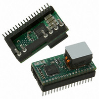
Manufacturer Part Number
NDM1-12-120
Description
DIG CONV DC/DC POL 0.6~2.5V 12A
Manufacturer
CUI Inc
Series
Novum NDM1-12r
Type
Digital Point of Load (POL) Non-Isolatedr
Datasheet
1.NDM1-12-120.pdf
(19 pages)
Specifications of NDM1-12-120
Output
0.6 ~ 2.5V
Number Of Outputs
1
Power (watts)
30W
Mounting Type
Through Hole
Voltage - Input
8.5 ~ 14V
Package / Case
24-DIP Module
1st Output
0.6 ~ 2.5 VDC @ 12A
Size / Dimension
0.93" L x 0.50" W x 0.46" H (23.6mm x 12.7mm x 11.7mm)
Power (watts) - Rated
30W
Efficiency
95%
Lead Free Status / RoHS Status
Lead free / RoHS Compliant
Operating Temperature
-
3rd Output
-
2nd Output
-
Other names
102-2140


MODEL:
SYNC FUNCTION
The NDM1-12 module achieved voltage regulation thru
digital pulse width modulation (DPWM). A
synchronization method is provided where multiple
slave devices are controlled by a single master device
via open loop phase alignment of the PWM patterns.
The DPWM synchronization allows the timing of the
pulse width modulation to be aligned between the
master and slave(s) at the same switching frequency
rate. The DPWM synchronization will prevent the de-
vices from drifting from each other with respect to the
start of the pulse width modulation. By default the
slave phase shift is 180° from the master.
Figure 4 illustrates the connectivity of the SYNC signal
for the case where two slave devices are used in a
master/slave configuration. This case shows the exam-
ple where several NDM1-12 modules are used to control
various voltage rails at the same switching frequency.
DPWM synchronization ensures that the starting points
of each slaves PWM patterns are under the control of
the designated master device and that the master and
slave on-chip oscillators are frequency locked to within
a certain error margin.
The slave device will check for slow and fast arriving
SYNC pulses and flag the error condition if enabled.
An error condition will cause an exit from master-slave
synchronization, resulting in the slave returning to
free-running PWM generation which is not aligned to
the master. The slave will again begin the synchroniza-
tion process. After all three stages of the synchroniza-
tion process are completed, the slave PWM will again be
synchronized to the master.
SYNC(Out)
Master
20050 SW 112
PWM2
PWM1
Figure 4: Block Diagram of Master-Slave
NDM1-12-120
Synchronization Connection
th
Ave. Tualatin, Oregon 97062
a division of CUI INC
SYNC (IN)
SYNC (IN)
Slave
Slave
PWM2
PWM1
PWM1
PWM2
DESCRIPTION:
phone 503.612.2300
OUTPUT VOLTAGE TRIMMING
As a digital POL module, the NDM1-12 module can be
programmed via PMBus command to different output
voltages without any hardware circuit board
modifications. The output voltage can also be trimmed
at the factory or via the V-Infinity GUI and stored in
non-volatile memory in the NDM1-12 module.
STARTUP DELAY AND RAMP UP TIME
POL startup delay and startup ramp up rate are
adjustable through GUI or PMBus commands. The
startup delay range is 0mS to 1048mS. The default
set up is 0mS. Ramp up rate ranges from 2.6V/mS to
10.13mV/mS. Ramp up is monolithic and default set up
is 1V/mS.
Figure 5: Adjustable range of startup delay and ramp
up rate.
NON-ISOLATED DIGITAL DC-DC
POL CONVERTER
Vout
fax 503.612.2382 www.novumdigital.com
0
Startup Delay
Max = 1.048 s,
Min = 0 s
Min = 10.13 mv/ms
Vout Ramp slope
Max = 2.6 v/ms,
Slope can be adjusted
date
page
Vout can be adjusted real time
with expected ramp rate
10/2010
12 of 19
t
Related parts for NDM1-12-120
Image
Part Number
Description
Manufacturer
Datasheet
Request
R

Part Number:
Description:
Digital Dc-dc Pol Converter
Manufacturer:
CUI INC
Datasheet:

Part Number:
Description:
DEMO NDM1 DC/DC 12A/25A MODULES
Manufacturer:
CUI Inc
Datasheet:

Part Number:
Description:
DIG CONV DC/DC POL 0.6~2.5V 25A
Manufacturer:
CUI Inc
Datasheet:
Part Number:
Description:
Digital Dc-dc Pol Converter
Manufacturer:
CUI INC
Datasheet:

Part Number:
Description:
CABLE ASSY LATCH 5PIN 5X22AWG 1'
Manufacturer:
CUI Inc
Datasheet:

Part Number:
Description:
CABLE ASSY LATCH 5PIN 5X22AWG 1'
Manufacturer:
CUI Inc
Datasheet:

Part Number:
Description:
CABLE SHLD LATCH 5PIN 24AWG 6'
Manufacturer:
CUI Inc
Datasheet:

Part Number:
Description:
LINE DRIVER CABLE FOR AMT-102 1M
Manufacturer:
CUI Inc
Datasheet:

Part Number:
Description:
LINE DRIVER CABLE FOR AMT-103 1M
Manufacturer:
CUI Inc
Datasheet:

Part Number:
Description:
CABLE SHLD MATING 5PIN 24AWG 6'
Manufacturer:
CUI Inc
Datasheet:

Part Number:
Description:
SPEAKER ALNICO 8OHM 2W 100MM SQR
Manufacturer:
CUI Inc
Datasheet:

Part Number:
Description:
ac-dc converter
Manufacturer:
CUI [CUI INC]
Datasheet:
Part Number:
Description:
MEDICAL SWITCHING POWER SUPPLY
Manufacturer:
CUI [CUI INC]
Datasheet:
Part Number:
Description:
DC-DC Converter
Manufacturer:
CUI [CUI INC]
Datasheet:
Part Number:
Description:
DC/DC Converter
Manufacturer:
CUI [CUI INC]
Datasheet: