NDM1-12-120 CUI Inc, NDM1-12-120 Datasheet - Page 13
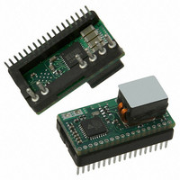
NDM1-12-120
Manufacturer Part Number
NDM1-12-120
Description
DIG CONV DC/DC POL 0.6~2.5V 12A
Manufacturer
CUI Inc
Series
Novum NDM1-12r
Type
Digital Point of Load (POL) Non-Isolatedr
Datasheet
1.NDM1-12-120.pdf
(19 pages)
Specifications of NDM1-12-120
Output
0.6 ~ 2.5V
Number Of Outputs
1
Power (watts)
30W
Mounting Type
Through Hole
Voltage - Input
8.5 ~ 14V
Package / Case
24-DIP Module
1st Output
0.6 ~ 2.5 VDC @ 12A
Size / Dimension
0.93" L x 0.50" W x 0.46" H (23.6mm x 12.7mm x 11.7mm)
Power (watts) - Rated
30W
Efficiency
95%
Lead Free Status / RoHS Status
Lead free / RoHS Compliant
Operating Temperature
-
3rd Output
-
2nd Output
-
Other names
102-2140


MODEL:
OUTPUT VOLTAGE SEQUENCING
The NDM1-12 can be configured to achieve advanced
voltage sequencing between power rails. This capability
eliminates the need for additional power management
circuitry, in a system environment with multiple voltage
domains. Ensuring consistent and predictable
start-up of multiple voltage rails after power-on or
power system reset (due to power outage or fault
condition) prevents catastrophic and unpredictable
current flows through digital processors and other
loads served.
Coordination of voltage rails and predictable shutdown
under fault conditions reduces the risk of unpredictable
system behavior where a problem occurs with one of
the voltage rails in a system application.
Programmable power-on sequencing delays may also
be used to ensure certain voltage rails are stabilized
before energizing mission critical functions.
A recommended configuration for multiple module
systems is shown in figure 6 where the control signal
is used to initiate sequencing during normal operations
and the FAULT signal is used for fault management.
Before the load systems are connected, it is necessary
to program the ON Rise Time, On Time Delay, and OFF
Time Delay for each module. This can be easily ac-
complished using the V-Infinity GUI which is the ideal
tool to program and fine tune these parameters during
development. In the Basic tab of the Configure section
of the GUI the ON Rise Time, On Time Delay, and OFF
Time Delay can all be independently set to meet system
requirements. Either positive or negative logic of the
CONTROL pin can be configured as required. Figure 7
illustrated the timing diagram for normal sequencing.
Upon assertion of the CONTROL pin the ON Time Delay
begins. The output voltage will begin to rise after the
ON Time Delay is over. The output voltage will rise
monotonically until reaching regulation. The amount
of time to reach regulation from the end of the ON
Time Delay is the On Rise Time. When the CONTROL
pin becomes unasserted the OFF Time Delay begins
and the output voltage will remain regulated until this
delay is over. The voltage ramp during turn-off is not
controlled by the module, but by the load current as it
discharges the output capacitance. Once the system
designer is satisfied with the timing sequence, the tim-
ing parameters can be permanently stored in the non-
20050 SW 112
NDM1-12-120
th
Ave. Tualatin, Oregon 97062
a division of CUI INC
DESCRIPTION:
phone 503.612.2300
volatile memory of the module.
For fault management, the FAULT pin of each module
can be tied together so that if there is a fault (Over
Voltage, Over Current, Input Under Voltage, or
Temperature) on any module in the system all units will
shut down immediately and remain off until the fault
condition is removed. The turn-off delays are ignored
in a fault condition and there is no ramp down control.
Module 1 Vout
Module 2 Vout
Module 3 Vout
CTRL = 0V
Figure 6: Multiple Module Configuration
NON-ISOLATED DIGITAL DC-DC
POL CONVERTER
fax 503.612.2382 www.novumdigital.com
On Time Delay
3.3V
Figure 7: Timing Diagram
On Rise Time
NDM1-12
NDM1-12
NDM1-12
date
page
Off Time Delay
10/2010
13 of 19
Related parts for NDM1-12-120
Image
Part Number
Description
Manufacturer
Datasheet
Request
R

Part Number:
Description:
Digital Dc-dc Pol Converter
Manufacturer:
CUI INC
Datasheet:

Part Number:
Description:
DEMO NDM1 DC/DC 12A/25A MODULES
Manufacturer:
CUI Inc
Datasheet:

Part Number:
Description:
DIG CONV DC/DC POL 0.6~2.5V 25A
Manufacturer:
CUI Inc
Datasheet:
Part Number:
Description:
Digital Dc-dc Pol Converter
Manufacturer:
CUI INC
Datasheet:

Part Number:
Description:
CABLE ASSY LATCH 5PIN 5X22AWG 1'
Manufacturer:
CUI Inc
Datasheet:

Part Number:
Description:
CABLE ASSY LATCH 5PIN 5X22AWG 1'
Manufacturer:
CUI Inc
Datasheet:

Part Number:
Description:
CABLE SHLD LATCH 5PIN 24AWG 6'
Manufacturer:
CUI Inc
Datasheet:

Part Number:
Description:
LINE DRIVER CABLE FOR AMT-102 1M
Manufacturer:
CUI Inc
Datasheet:

Part Number:
Description:
LINE DRIVER CABLE FOR AMT-103 1M
Manufacturer:
CUI Inc
Datasheet:

Part Number:
Description:
CABLE SHLD MATING 5PIN 24AWG 6'
Manufacturer:
CUI Inc
Datasheet:

Part Number:
Description:
SPEAKER ALNICO 8OHM 2W 100MM SQR
Manufacturer:
CUI Inc
Datasheet:

Part Number:
Description:
ac-dc converter
Manufacturer:
CUI [CUI INC]
Datasheet:
Part Number:
Description:
MEDICAL SWITCHING POWER SUPPLY
Manufacturer:
CUI [CUI INC]
Datasheet:
Part Number:
Description:
DC-DC Converter
Manufacturer:
CUI [CUI INC]
Datasheet:
Part Number:
Description:
DC/DC Converter
Manufacturer:
CUI [CUI INC]
Datasheet: