C8051T606ZDB Silicon Laboratories Inc, C8051T606ZDB Datasheet - Page 17
C8051T606ZDB
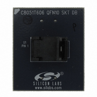
Manufacturer Part Number
C8051T606ZDB
Description
CARD DAUGHTER QFN10 SOCKET
Manufacturer
Silicon Laboratories Inc
Datasheets
1.C8051T600EDB.pdf
(188 pages)
2.C8051T606TDB.pdf
(1 pages)
3.C8051T606TDB.pdf
(14 pages)
Specifications of C8051T606ZDB
Module/board Type
Socket Module - QFN
Maximum Operating Temperature
+ 85 C
Minimum Operating Temperature
- 40 C
Lead Free Status / RoHS Status
Lead free / RoHS Compliant
For Use With/related Products
C8051T606
Lead Free Status / Rohs Status
Lead free / RoHS Compliant
Other names
336-1668


3. Pin Definitions
Table 3.1. Pin Definitions for the C8051T600/1/2/3/4/5
CNVSTR
EXTCLK
Name
C2CK
P0.7 /
P0.0 /
VREF
P0.2 /
P0.3 /
P0.6 /
RST /
GND
P0.4
P0.5
C2D
P0.1
V
V
NC
DD
PP
QFN11
Pin
10
11
—
3
8
1
2
4
5
6
7
9
SOIC14
4,9,11
Pin
14
10
12
13
7
3
2
5
6
8
1
D I/O or
D I/O or
D I/O or
D I/O or
D I/O or
D I/O or
D I/O or
D I/O or
A I/O or
D I/O
D I/O
D I/O
Type
D In
D In
A In
A In
A In
A In
A In
A In
A In
A In
A In
A In
Description
Power Supply Voltage.
Ground.
Device Reset. Open-drain output of internal POR or V
Clock signal for the C2 Debug Interface.
Port 0.7.
Bi-directional data signal for the C2 Debug Interface.
Port 0.0.
External VREF input.
Port 0.1.
Port 0.2.
V
Port 0.3.
External Clock Pin. This pin can be used as the external clock
input for CMOS, capacitor, or RC oscillator configurations.
Port 0.4.
Port 0.5.
Port 0.6.
ADC0 External Convert Start Input.
No Connection.
PP
Programming Supply Voltage.
Rev. 1.2
C8051T600/1/2/3/4/5/6
DD
monitor.
17
Related parts for C8051T606ZDB
Image
Part Number
Description
Manufacturer
Datasheet
Request
R

Part Number:
Description:
SMD/C°/SINGLE-ENDED OUTPUT SILICON OSCILLATOR
Manufacturer:
Silicon Laboratories Inc
Part Number:
Description:
Manufacturer:
Silicon Laboratories Inc
Datasheet:
Part Number:
Description:
N/A N/A/SI4010 AES KEYFOB DEMO WITH LCD RX
Manufacturer:
Silicon Laboratories Inc
Datasheet:
Part Number:
Description:
N/A N/A/SI4010 SIMPLIFIED KEY FOB DEMO WITH LED RX
Manufacturer:
Silicon Laboratories Inc
Datasheet:
Part Number:
Description:
N/A/-40 TO 85 OC/EZLINK MODULE; F930/4432 HIGH BAND (REV E/B1)
Manufacturer:
Silicon Laboratories Inc
Part Number:
Description:
EZLink Module; F930/4432 Low Band (rev e/B1)
Manufacturer:
Silicon Laboratories Inc
Part Number:
Description:
I°/4460 10 DBM RADIO TEST CARD 434 MHZ
Manufacturer:
Silicon Laboratories Inc
Part Number:
Description:
I°/4461 14 DBM RADIO TEST CARD 868 MHZ
Manufacturer:
Silicon Laboratories Inc
Part Number:
Description:
I°/4463 20 DBM RFSWITCH RADIO TEST CARD 460 MHZ
Manufacturer:
Silicon Laboratories Inc
Part Number:
Description:
I°/4463 20 DBM RADIO TEST CARD 868 MHZ
Manufacturer:
Silicon Laboratories Inc
Part Number:
Description:
I°/4463 27 DBM RADIO TEST CARD 868 MHZ
Manufacturer:
Silicon Laboratories Inc
Part Number:
Description:
I°/4463 SKYWORKS 30 DBM RADIO TEST CARD 915 MHZ
Manufacturer:
Silicon Laboratories Inc
Part Number:
Description:
N/A N/A/-40 TO 85 OC/4463 RFMD 30 DBM RADIO TEST CARD 915 MHZ
Manufacturer:
Silicon Laboratories Inc
Part Number:
Description:
I°/4463 20 DBM RADIO TEST CARD 169 MHZ
Manufacturer:
Silicon Laboratories Inc