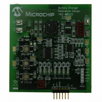
MCP1631RD-MCC2 Microchip Technology, MCP1631RD-MCC2 Datasheet
MCP1631RD-MCC2
Specifications of MCP1631RD-MCC2


Related parts for MCP1631RD-MCC2


MCP1631RD-MCC2 Summary of contents
Page 1
... LED Lighting Applications • Constant Current SEPIC Power Train Design • USB Input Programmable Switching Battery Chargers © 2008 Microchip Technology Inc. General Description T he MCP16 31/MC P1631 gh-spe ed analog pulse width modulator (PWM) used to develop intelligent power systems. When combined with a ...
Page 2
... V 1 EXT SHDN VDD 18 CS/V OSC 3 RAMP OSC 4 DIS COMP OUT REF OUT GND VDD_IN Lead 4x4 QFN MCP1631/MCP1631V 20 V EXT 19 P VDD 18 CS/V RAMP 17 FB COMP OUT 14 VS OUT VDD_OUT P GND V EXT P VDD NC CS/V RAMP © 2008 Microchip Technology Inc. ...
Page 3
... VDD OSC OUT SHDN OSC COMP VS A GND PIC12F683 V GP1/C DD CCP1 GP3 GP4 GP5 GND GP0/C © 2008 Microchip Technology Inc. MCP1631/HV/MCP1631V/VHV Multi-cell, Multi-Chemistry Charger SCHOTTKY C C DIODE L1A L1B EXT CS GND REF DIS OUT R R THERM C OUT C A VDD_OUT DS22063B-page 3 ...
Page 4
... Options Only; For MCP1631 and MCP1631V AV V Internal DD 1.2V V REF V DD Overvoltage Comp - w/ Hysteresis C2 + OSC DIS 100 kΩ 0.1 µA UVLO Remove for MCP1631V R and MCP1631VHV Options . DD is input DD_IN P VDD OT V EXT P GND 100 kΩ 10R OUT OUT © 2008 Microchip Technology Inc. ...
Page 5
... Dropout voltage is defined as the input to output differential at which the output voltage drops 2% below its measured value with an applied input voltage of V © 2008 Microchip Technology Inc. MCP1631/HV/MCP1631V/VHV † Notice: Stresses above those listed under "Maximum Ratings" may cause permanent damage to the device. This is ...
Page 6
... IN MHz 5V 1.2V, IN REF V = 1.4V 2.0V FB COMP 5V 1.2V, IN REF V = 1.0V 2.0V, FB COMP Absolute Value mV µ 3.0V to 5.0V 0.12V GAIN = 10 V kΩ / 100 mV < V < 100 mV, OUT +0.12V kΩ µ DROPOUT(MAX) = highest voltage measured over the . OUT © 2008 Microchip Technology Inc. ...
Page 7
... TCV 5: Dropout voltage is defined as the input to output differential at which the output voltage drops 2% below its measured value with an applied input voltage of V © 2008 Microchip Technology Inc. MCP1631/HV/MCP1631V/VHV = 3.0V to 5.5V MHz with 10% Duty Cycle, C ...
Page 8
... OUT + 3.0V to 5.5V Units Conditions °C Steady State °C °C Transient °C/W Typical 4 Layer board with interconnecting vias °C/W Typical 4 Layer board with interconnecting vias °C/W Typical 4 Layer board with interconnecting vias © 2008 Microchip Technology Inc. , ...
Page 9
... +3.3V 3. +3.0V DD 3.00 2.80 Ambient Temperature (°C) FIGURE 2-3: Input Quiescent Current vs. Temperature. © 2008 Microchip Technology Inc. MCP1631/HV/MCP1631V/VHV = 1 MHz with 10% Duty Cycle, C OSC 4.00 3.70 3.40 3.10 2.80 2.50 2.20 1.90 1.60 1.30 1.00 FIGURE 2-4: Temperature (MCP1631/MCP1631V). ...
Page 10
... FIGURE 2-11: vs. Temperature +5. FIGURE 2-12: Low vs. Temperature. = 0.1 µ +3. +3. +4. +5. +5.5V DD Ambient Temperature (°C) V Fall Time vs. EXT V = +5. +5. +3. +3. +4.0V DD Ambient Temperature (°C) Amplifier A1 Offset Voltage V = +5. +5. +4. +3. +3.0V DD Ambient Temperature (°C) Amplifier A1 Output Voltage © 2008 Microchip Technology Inc. ...
Page 11
... Ambient Temperature (°C) FIGURE 2-14: Amplifier A1 Source Current vs. Temperature. 1 +5.5V DD 1.4 1 +5. +4. +3.3V 0 +3.0V DD 0.4 Ambient Temperature (°C) FIGURE 2-15: Amplifier A2 Offset Voltage vs. Temperature. © 2008 Microchip Technology Inc. MCP1631/HV/MCP1631V/VHV = 1 MHz with 10% Duty Cycle, C OSC FIGURE 2-16: Low vs. Temperature +3. +5. +5. FIGURE 2-17: vs ...
Page 12
... FIGURE 2-24: MCP1631VHV V = 0.1 µ +5. +5. +3. +3. +4.0V DD Ambient Temperature (°C) Amplifier A3 Source Current V = +5. +5. +4. +3. +3.3V DD Ambient Temperature (°C) MCP1631 and MCP1631HV V = +5.0V DD Ambient Temperature (°C) MCP1631V and Max Voltage (V). RAMP © 2008 Microchip Technology Inc. ...
Page 13
... V = +4.0V DD 0.030 V = +3.0V V 0.020 DD DD 0.010 0.000 Ambient Temperature (°C) FIGURE 2-27: Overvoltage Threshold Hysteresis (V) vs. Temperature. © 2008 Microchip Technology Inc. MCP1631/HV/MCP1631V/VHV = 1 MHz with 10% Duty Cycle, C OSC 1.7 1.6 1 +4.0V DD 1.4 1.3 1.2 1.1 1.0 0.9 0.8 FIGURE 2-28: Threshold (V) vs ...
Page 14
... Temperature (°C) LDO Line Regulation vs. V =5. =6. 100 mV p-p INAC C =0 μ =100 µA OUT 0 100 1000 Frequency (kHz) LDO PSRR vs. Frequency 5.0V 6.0V OUT 100 1000 Frequency (kHz) LDO Output Noise vs. © 2008 Microchip Technology Inc. ...
Page 15
... Oscillator Input (OSC IN External Oscillator Input, used to set power train switching frequency and maximum duty cycle, V enabled while low and disabled while high. © 2008 Microchip Technology Inc. MCP1631/HV/MCP1631V/VHV Table 3-1. Sym P Power ground return ...
Page 16
... Exposed Thermal Pad (EP) and the A ) must be connected to the same potential on the Printed OUT Circuit Board (PCB). connect to ) OUT ) RAMP input for voltage mode PWM control. ) VDD gate drive supply input, connect EXT ) EXT . VDD pin; they GND © 2008 Microchip Technology Inc. ...
Page 17
... P source of 5V. Typical output power using the V output to directly drive the external MOSFET can exceed 50W depending upon application and switching frequency. © 2008 Microchip Technology Inc. MCP1631/HV/MCP1631V/VHV 4.4 Current Sense Amplifier (A2) The A2 current sense amplifier is used to sense current in the secondary side of a SEPIC converter or freewheeling current in a Buck converter ...
Page 18
... MCP1631/HV/MCP1631V/VHV NOTES: DS22063B-page 18 © 2008 Microchip Technology Inc. ...
Page 19
... The input or primary inductor and output or secondary inductor are typically constructed from a single magnetic device with two windings, this is commonly referred coupled inductor. Using coupled © 2008 Microchip Technology Inc. MCP1631/HV/MCP1631V/VHV inductors has significant advantages in addition to the size and cost benefits of a single core with multiple windings ...
Page 20
... VS A GND PIC12F683 V GP1/C DD CCP1 GP4 GND GP0/C FIGURE 5-1: +5V ac-dc or USB Input Application. DS22063B-page 20 output. This Multi-cell Multi-Chemistry Charger SCHOTTKY C C DIODE L1A L1B EXT CS GND REF DIS OUT R GP3 GP5 R THERM C OUT C A VDD_OUT © 2008 Microchip Technology Inc. ...
Page 21
... IS OV OUT SHDN NC OSC COMP A VS GND PIC12F683 V GP1/C DD CCP1 GP3 GP4 GP5 GND GP0/C FIGURE 5-2: +5.5V to +16.0V Input. © 2008 Microchip Technology Inc. MCP1631/HV/MCP1631V/VHV Multi-cell Multi-Chemistry Charger SCHOTTKY C C DIODE L1A L1B EXT REF DIS OUT R R THERM C OUT C ...
Page 22
... COMP VS A GND PIC12F683 V GP1/C DD CCP1 GP3 GP4 GND GP0/C FIGURE 5-3: Wide Range High Voltage Input. DS22063B-page 22 Multi-cell Multi-Chemistry Charger SCHOTTKY C C DIODE L1A L1B EXT CS GND REF DIS OUT R GP5 R THERM C OUT C A VDD_OUT © 2008 Microchip Technology Inc. ...
Page 23
... Note: In the event the full Microchip part number cannot be marked on one line, it will be carried over to the next line, thus limiting the number of available characters for customer-specific information. © 2008 Microchip Technology Inc. MCP1631/HV/MCP1631V/VHV Example: Example: Example: ...
Page 24
... MCP1631/HV/MCP1631V/VHV /HDG 3ODVWLF 4XDG )ODW 1R /HDG 3DFNDJH 0/ ± 1RWH 1RWHV DS22063B-page 24 PP %RG\ >4)1@ © 2008 Microchip Technology Inc. ...
Page 25
... Microchip Technology Inc. MCP1631/HV/MCP1631V/VHV DS22063B-page 25 ...
Page 26
... MCP1631/HV/MCP1631V/VHV /HDG 3ODVWLF 6KULQN 6PDOO 2XWOLQH 66 ± 1RWH 1RWHV DS22063B-page 26 PP %RG\ >6623@ I © 2008 Microchip Technology Inc. φ ...
Page 27
... Microchip Technology Inc. MCP1631/HV/MCP1631V/VHV PP %RG\ >76623@ I φ DS22063B-page 27 ...
Page 28
... MCP1631/HV/MCP1631V/VHV NOTES: DS22063B-page 28 © 2008 Microchip Technology Inc. ...
Page 29
... Section 2.0 “Typical Performance Curves”, Input Offset Voltage: changed minimum, typical, maximum from -0.6, -, +0.6 to -5, -0.6, +5, respectively; 2. Updated Section 6.0 “Packaging Informa- tion”; 3. Updated the Product Identification System. Revision A (October 2007) • Original Release of this Document. © 2008 Microchip Technology Inc. MCP1631/HV/MCP1631V/VHV DS22063B-page 29 ...
Page 30
... MCP1631/HV/MCP1631V/VHV NOTES: DS22063B-page 30 © 2008 Microchip Technology Inc. ...
Page 31
... Package ML = Plastic Quad Flat, No Lead (4x4x0.9), 20-lead SS = Plastic Shrink Small Outline (5.30 mm), 20-lead ST = Plastic Thin Shrink Small Outline (4.4 mm), 20-Lead * All package offerings are Pb Free (Lead Free) © 2008 Microchip Technology Inc. MCP1631/HV/MCP1631V/VHV X /XX Examples: Package a) MCP1631-E/ML: b) MCP1631-E/SS: c) MCP1631-E/ST: ...
Page 32
... MCP1631/HV/MCP1631V/VHV NOTES: DS22063B-page 32 © 2008 Microchip Technology Inc. ...
Page 33
... PowerMate, PowerTool, REAL ICE, rfLAB, Select Mode, Total Endurance, WiperLock and ZENA are trademarks of Microchip Technology Incorporated in the U.S.A. and other countries. SQTP is a service mark of Microchip Technology Incorporated in the U.S.A. All other trademarks mentioned herein are property of their respective companies. ...
Page 34
... Fax: 886-3-572-6459 Taiwan - Kaohsiung Tel: 886-7-536-4818 Fax: 886-7-536-4803 Taiwan - Taipei Tel: 886-2-2500-6610 Fax: 886-2-2508-0102 Thailand - Bangkok Tel: 66-2-694-1351 Fax: 66-2-694-1350 © 2008 Microchip Technology Inc. EUROPE Austria - Wels Tel: 43-7242-2244-39 Fax: 43-7242-2244-393 Denmark - Copenhagen Tel: 45-4450-2828 Fax: 45-4485-2829 France - Paris Tel: 33-1-69-53-63-20 ...