MCP1631RD-MCC2 Microchip Technology, MCP1631RD-MCC2 Datasheet - Page 5
MCP1631RD-MCC2
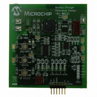
Manufacturer Part Number
MCP1631RD-MCC2
Description
REFERENCE DESIGN MCP1631HV
Manufacturer
Microchip Technology
Datasheets
1.MCP1631VHVT-330EST.pdf
(34 pages)
2.MCP1631HV-330EST.pdf
(54 pages)
3.MCP1631RD-MCC2.pdf
(20 pages)
4.MCP1631RD-MCC2.pdf
(328 pages)
Specifications of MCP1631RD-MCC2
Main Purpose
Power Management, Battery Charger
Embedded
Yes, MCU, 8-Bit
Utilized Ic / Part
MCP1631HV, PIC16F883
Primary Attributes
1 ~ 2 Cell- Li-Ion, 1 ~ 5 Cell- NiCd/NiMH, 1 ~ 2 1W LEDs
Secondary Attributes
Status LEDs
Silicon Manufacturer
Microchip
Application Sub Type
Battery Charger
Kit Application Type
Power Management - Battery
Silicon Core Number
MCP1631HV, PIC16F883
Kit Contents
Board
Lead Free Status / RoHS Status
Lead free / RoHS Compliant
Lead Free Status / RoHS Status
Lead free / RoHS Compliant


1.0
Absolute Maximum Ratings †
V
V
All Other I/O ..............................(GND - 0.3V) to (V
LX to GND............................................. -0.3V to (V
V
Storage temperature .....................................-65°C to +150°C
Maximum Junction Temperature ...................-40°C to +150°C
Operating Junction Temperature...................-40°C to +125°C
ESD Protection On All Pins:
HBM ................................................................................. 4 kV
MM ..................................................................................400V
DC CHARACTERISTICS
© 2008 Microchip Technology Inc.
Electrical Specifications: Unless otherwise noted, V
V
Input Characteristics
Input Voltage (MCP1631/V)
Input Voltage
(MCP1631HV/VHV)
Undervoltage Lockout
(MCP1631/V)
Undervoltage Lockout Hysteresis
(MCP1631/MCP1631V)
Input Quiescent Current
(MCP1631/V, MCP1631HV,VHV)
Shutdown Current
I_AVDD for MCP1631/V
I_VIN for MCP1631HV/VHV
OSC
Low Level Input Voltage
High Level Input Voltage
Input Leakage Current
External Oscillator Range
Minimum Oscillator High Time
Minimum Oscillator Low Time
Oscillator Rise and Fall Time
Oscillator Input Capacitance
Note 1:
IN
IN
EXT
DD
- GND (MCP1631/V)................................................+6.5V
- GND (MCP1631HV/VHV)....................................+18.0V
Output Short Circuit Current ........................ Continuous
for typical values = 5.0V, T
IN
, OSC
2:
3:
4:
5:
ELECTRICAL
CHARACTERISTICS
Parameters
External Oscillator Input (OSC
characterization testing. Signal levels between 0.8V and 2.0V with rise and fall times measured between 10% and 90%
of maximum and minimum values. Not production tested. Additional timing specifications were fully characterized and
specified that are not production tested.
The minimum V
TCV
temperature range. V
Load regulation is measured at a constant junction temperature using low duty cycle pulse testing. Changes in output
voltage due to heating effects are determined using thermal regulation specification TCV
Dropout voltage is defined as the input to output differential at which the output voltage drops 2% below its measured
value with an applied input voltage of V
DIS
and SHDN Input Levels
OUT
= (V
OUT-HIGH
IN
must meet two conditions: V
A
for typical values = +25°C, T
OUT-LOW
- V
T
T
UVLO
T
OH
OL
I
OUT-LOW
R
IN_SHDN
UVLO
I(V
C
I
F
Sym
_MIN.
V
V
_MIN.
LEAK
and T
V
V
OSC
OSC
DD
DD
IH
IL
IN
_HYS
IN
= lowest voltage measured over the temperature range.
)
) rise and fall times between 10 ns and 10 µs were determined during device
F
) *10
DD
DD
6
OUT(MAX)
/ (V
+ 0.3V)
+ 0.3V)
MCP1631/HV/MCP1631V/VHV
IN
0.01
Min
3.0
3.5
2.7
2.0
40
—
—
—
—
—
—
= 3.0V to 5.5V, F
R
* ΔTemperature), V
IN
+ V
A
≥ 3.5V and V
= -40°C to +125°C for all minimum and maximums.
DROPOUT(MAX)
0.005
Typ
2.8
3.7
2.4
4.4
64
10
—
—
—
—
—
—
5
† Notice: Stresses above those listed under "Maximum
Ratings" may cause permanent damage to the device. This is
a stress rating only and functional operation of the device at
those or any other conditions above those indicated in the
operational sections of this specification is not intended.
Exposure to maximum rating conditions for extended periods
may affect device reliability.
OSC
IN
≥ (V
OUT-HIGH
= 1 MHz with 10% Duty Cycle, C
Max
16.0
100
5.5
3.0
0.8
or 3.5V, whichever is greater.
12
17
10
—
—
—
5
1
2
OUT(MAX)
= highest voltage measured over the
Units
MHz
mV
mA
µA
µA
µA
ns
µs
pf
V
V
V
V
V
+ V
DROPOUT(MAX)
Non-HV Options
HV Options (Note 2)
V
below UVLO threshold
UVLO Hysteresis
SHDN = V
SHDN = GND =OSC
Note: Amplifier A3 remains
powered during Shutdown.
Maximum operating frequency is
dependent upon circuit topology
and duty cycle.
Note 1
IN
OUT
Falling, V
.
DD
Conditions
).
EXT
IN
=OSC
= 0.1 µF,
DS22063B-page 5
low when input
DIS
DIS
,
Related parts for MCP1631RD-MCC2
Image
Part Number
Description
Manufacturer
Datasheet
Request
R

Part Number:
Description:
REFERENCE DESIGN FOR MCP1631HV
Manufacturer:
Microchip Technology
Datasheet:

Part Number:
Description:
REF DES BATT CHARG OR LED DRIVER
Manufacturer:
Microchip Technology
Datasheet:

Part Number:
Description:
Manufacturer:
Microchip Technology Inc.
Datasheet:
Part Number:
Description:
Manufacturer:
Microchip Technology Inc.
Datasheet:
Part Number:
Description:
Manufacturer:
Microchip Technology Inc.
Datasheet:
Part Number:
Description:
Manufacturer:
Microchip Technology Inc.
Datasheet:
Part Number:
Description:
Manufacturer:
Microchip Technology Inc.
Datasheet:
Part Number:
Description:
Manufacturer:
Microchip Technology Inc.
Datasheet:
Part Number:
Description:
Manufacturer:
Microchip Technology Inc.
Datasheet:
Part Number:
Description:
Manufacturer:
Microchip Technology Inc.
Datasheet: