EVAL-ADM1176EBZ Analog Devices Inc, EVAL-ADM1176EBZ Datasheet - Page 13
EVAL-ADM1176EBZ
Manufacturer Part Number
EVAL-ADM1176EBZ
Description
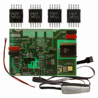
BOARD EVALUATION FOR ADM1176
Manufacturer
Analog Devices Inc
Specifications of EVAL-ADM1176EBZ
Main Purpose
Power Management, Hot Swap Controller
Embedded
No
Utilized Ic / Part
ADM1176
Primary Attributes
Hot Swap Controller, Digital Power Monitor, High Side MOSFET Driver
Secondary Attributes
SMBus, I2C, 3.15 V ~ 16.5 V Supply
Lead Free Status / RoHS Status
Lead free / RoHS Compliant


OVERVIEW OF THE HOT SWAP FUNCTION
When circuit boards are inserted into a live backplane, discharged
supply bypass capacitors draw large transient currents from the
backplane power bus as they charge. Such transient currents can
cause permanent damage to connector pins, as well as dips on
the backplane supply that can reset other boards in the system.
The ADM1176 is designed to turn a circuit board supply voltage on
and off in a controlled manner, allowing the circuit board to be
safely inserted into or removed from a live backplane. The
ADM1176 can reside either on the backplane or on the circuit
board itself.
The ADM1176 controls the inrush current to a fixed maximum
level by modulating the gate of an external N-channel FET placed
between the live supply rail and the load. This hot swap function
protects the card connectors and the FET itself from damage and
limits any problems that can be caused by high current loads on
the live supply rail.
The ADM1176 holds the GATE pin down (and therefore holds
off the FET) until certain conditions are met. An undervoltage
lockout circuit ensures that the device is provided with an adequate
input supply voltage. After the input supply voltage is successfully
detected, the device goes through an initial timing cycle to provide
a delay before it attempts a hot swap. This delay ensures that the
board is fully seated in the backplane before the board is
powered up.
After the initial timing cycle is complete, the hot swap function
is switched on under control of the ON pin. When the ON pin
is asserted high, the hot swap operation starts.
The ADM1176 charges up the gate of the FET to turn on the
load. It continues to charge up the GATE pin until the linear
current limit (set to 100 mV/R
nations of low load capacitance and high current limit, this limit
may not be reached before the load is fully charged up. If the
current limit is reached, the ADM1176 regulates the GATE pin
to keep the current at this limit. For currents above the overcurrent
fault timing threshold, nominally 100 mV/R
is timed by sourcing a current to the TIMER pin. If the load
becomes fully charged before the fault current limit time elapses
(when the TIMER pin reaches 1.3 V), the current drops below
the overcurrent fault timing threshold. The ADM1176 then
continues to further charge up the GATE pin to fully enhance the
FET for lowest R
If the fault current limit time is reached before the load drops
below the current limit, a fault has been detected, and the hot
swap operation is aborted by pulling down the GATE pin to
turn off the FET.
ON
, and the TIMER pin is pulled down again.
SENSE
) is reached. For some combi-
SENSE
, the current fault
Rev. B | Page 13 of 24
The ADM1176-2 immediately latches off and attempts a hot swap
only when the ON pin is deasserted and then asserted again. The
ADM1176-1, however, retries the hot swap operation indefinitely,
keeping the FET in its safe operating area (SOA) by using the
TIMER pin to time a cooldown period between hot swap attempts.
The current and voltage threshold combinations on the TIMER pin
set the retry duty cycle to 3.8%. The ADM1176 is designed to
operate over a range of supplies from 3.15 V to 16.5 V.
UNDERVOLTAGE LOCKOUT
An internal undervoltage lockout (UVLO) circuit resets the
ADM1176 if the voltage on the VCC pin is too low for normal
operation. The UVLO has a low-to-high threshold of 2.8 V, with
80 mV hysteresis. When there is a supply voltage greater than
2.8 V, the ADM1176 starts the initial timing cycle.
ON FUNCTION
The ADM1176-1 has an active high ON pin. The ON pin is the
input to a comparator that has a low-to-high threshold of 1.3 V,
a 50 mV hysteresis, and a glitch filter of 3 μs. A low input on the
ON pin turns off the hot swap operation by pulling the GATE pin
to ground, turning off the external FET. The TIMER pin is also
reset by turning on a pull-down current on this pin. A low-to-
high transition on the ON pin starts the hot swap operation.
A 10 kΩ pull-up resistor connecting the ON pin to the supply
is recommended.
Alternatively, an external resistor divider at the ON pin can be
used to program an undervoltage lockout value that is higher
than the internal UVLO circuit, thereby setting the hot swap
operation to start at a specific voltage level on the VCC pin. An
RC filter can be added at the ON pin to increase the delay time
at card insertion if the initial timing cycle delay is insufficient.
TIMER FUNCTION
The TIMER pin handles several timing functions with an
external capacitor, C
V
sources are a 5 μA pull-up, a 60 μA pull-up, a 2 μA pull-down,
and a 100 μA pull-down. The 100 μA pull-down is a nonideal
current source approximating a 7 kΩ resistor below 0.4 V.
These current and voltage levels, together with the value of C
chosen by the user, determine the initial timing cycle time, the
fault current limit time, and the hot swap retry duty cycle.
TIMERH
(1.3 V) and V
TIMER
TIMERL
. There are two comparator thresholds:
(0.2 V). The four timing current
ADM1176
TIMER
Related parts for EVAL-ADM1176EBZ
Image
Part Number
Description
Manufacturer
Datasheet
Request
R


Part Number:
Description:
BOARD EVAL FOR SI270X-A
Manufacturer:
Silicon Laboratories Inc
Datasheet:

Part Number:
Description:
BUCK CONV REF DESIGN KIT IP1201
Manufacturer:
International Rectifier
Datasheet:
Part Number:
Description:
BOARD DEMO SYNC DUAL BUCK CNVTER
Manufacturer:
International Rectifier
Datasheet:
Part Number:
Description:
BOARD DEMO SYNC BUCK CONVETER
Manufacturer:
International Rectifier
Datasheet:

Part Number:
Description:
EVALBOARD/EB Omnidirectional microphone - Analog
Manufacturer:
Analog Devices
Datasheet:
Part Number:
Description:
EVALBOARD/EB Omnidirectional microphone - Analog
Manufacturer:
Analog Devices
Datasheet:


Part Number:
Description:
BOARD EVAL LED DRIVER LT3756
Manufacturer:
Linear Technology
Datasheet:

Part Number:
Description:
BOARD EVAL FOR AD7741/7742
Manufacturer:
Analog Devices Inc
Datasheet:

Part Number:
Description:
±1.7g Dual-Axis IMEMS Accelerometer Evaluation Board
Manufacturer:
Analog Devices Inc
Datasheet:

Part Number:
Description:
IC MULTIPLIER ANALOG 8-SOIC T/R
Manufacturer:
Analog Devices Inc
Datasheet:

Part Number:
Description:
IC ANALOG MULTIPLIER 8-DIP
Manufacturer:
Analog Devices Inc
Datasheet:
Part Number:
Description:
IC ANALOG MULTIPLIER 8-SOIC
Manufacturer:
Analog Devices Inc
Datasheet:
Part Number:
Description:
IC ANALOG MULTIPLIER 8-DIP
Manufacturer:
Analog Devices Inc
Datasheet: