EVAL-ADM1176EBZ Analog Devices Inc, EVAL-ADM1176EBZ Datasheet - Page 14
EVAL-ADM1176EBZ
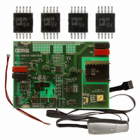
Manufacturer Part Number
EVAL-ADM1176EBZ
Description
BOARD EVALUATION FOR ADM1176
Manufacturer
Analog Devices Inc
Specifications of EVAL-ADM1176EBZ
Main Purpose
Power Management, Hot Swap Controller
Embedded
No
Utilized Ic / Part
ADM1176
Primary Attributes
Hot Swap Controller, Digital Power Monitor, High Side MOSFET Driver
Secondary Attributes
SMBus, I2C, 3.15 V ~ 16.5 V Supply
Lead Free Status / RoHS Status
Lead free / RoHS Compliant


ADM1176
GATE AND TIMER FUNCTIONS DURING
A HOT SWAP OPERATION
During hot insertion of a board onto a live supply rail at VCC,
the abrupt application of supply voltage charges the external
FET drain/gate capacitance, which can cause an unwanted gate
voltage spike. An internal circuit holds GATE low before the
internal circuitry wakes up. This substantially reduces the FET
current surges at insertion. The GATE pin is also held low
during the initial timing cycle until the ON pin is taken high to
start the hot swap operation.
During a hot swap operation, the GATE pin is first pulled up by
a 12.5 μA current source. If the current through the sense resistor
reaches the overcurrent fault timing threshold (V
up current of 60 μA on the TIMER pin is turned on and the
GATE pin starts charging up. At a slightly higher voltage in the
sense resistor, the error amplifier servos the GATE pin to maintain
a constant current to the load by controlling the voltage across
the sense resistor to the linear current limit, V
A normal hot swap operation is complete when the board supply
capacitors near full charge and the current through the sense
resistor drops to eventually reach the level of the board load
current. As soon as the current drops below the overcurrent
fault timing threshold, the current into the TIMER pin switches
from being a 60 μA pull-up to being a 100 μA pull-down. The
ADM1176 then drives the GATE voltage as high as it can to
fully enhance the FET and reduce R
A hot swap operation fails if the load current does not drop
below the overcurrent fault timing threshold, V
TIMER pin has charged up to 1.3 V. In this case, the GATE pin
is then pulled down with a 1.5 mA to 7 mA current sink (this varies
with supply voltage). The GATE pull-down stays on until a hot
swap retry starts, which can be forced by deasserting and then
reasserting the ON pin. On the ADM1176-1, the device retries a
hot swap operation automatically after a cooldown period.
The ADM1176 also features a method of protection from
sudden load current surges, such as a low impedance fault,
when the current seen across the sense resistor may go well
beyond the linear current limit. If the fast overcurrent trip
threshold, V
down is turned on immediately. This pulls the GATE voltage
down quickly to enable the ADM1176 to limit the length of the
current spike that passes through the external FET and to bring
the current through the sense resistor back into linear regulation as
quickly as possible. This process protects the backplane supply
from sustained overcurrent conditions that can otherwise cause
the backplane supply to droop during the overcurrent event.
OCFAST
, is exceeded, the 1.5 mA to 7 mA GATE pull-
ON
losses to a minimum.
OCTRIM
LIM
.
OCTRIM
, before the
), a pull-
Rev. B | Page 14 of 24
CALCULATING CURRENT LIMITS AND FAULT
CURRENT LIMIT TIME
The nominal linear current limit is determined by a sense
resistor connected between the VCC pin and the SENSE pin
as given by Equation 1.
The minimum linear fault current is given by Equation 2.
The maximum linear fault current is given by Equation 3.
The power rating of the sense resistor should be rated at the
maximum linear fault current level.
The minimum overcurrent fault timing threshold current is
given by Equation 4.
The maximum fast overcurrent trip threshold current is given
by Equation 5.
The fault current limit time is the time that a device spends
timing an overcurrent fault. The fault current limit time is given
by Equation 6.
INITIAL TIMING CYCLE
When VCC is first connected to the backplane supply, the
internal supply (Time Point 1 in Figure 30) of the ADM1176
must be charged up. A very short time later (significantly less
than 1 ms), the internal supply is fully up and, because the
undervoltage lockout voltage is exceeded at VCC, the device
comes out of reset. During this first short reset period, the
GATE pin is held down with a 25 mA pull-down current, and
the TIMER pin is pulled down with a 100 μA current sink.
The ADM1176 then goes through an initial timing cycle. At
Time Point 2, the TIMER pin is pulled high with 5 μA. At Time
Point 3, the TIMER reaches the V
portion of the initial cycle ends. The 100 μA current source then
pulls down the TIMER pin until it reaches 0.2 V at Time Point 4.
The initial cycle delay (Time Point 2 to Time Point 4) is related
to C
TIMER
I
I
I
I
I
t
t
FAULT
INITIAL
LIMIT(NOM)
LIMIT(MIN)
LIMIT(MAX)
OCTRIM(MIN)
OCFAST(MAX)
as shown in Equation 7.
≈ 21.7 × C
≈ 270 × C
= V
= V
= V
= V
= V
LIM(MIN)
LIM(MAX)
LIM(NOM)
OCTRIM(MIN)
OCFAST(MAX)
TIMER
TIMER
/R
/R
/R
ms/μF
ms/μF
SENSE(MAX)
SENSE(MIN)
SENSE
/R
/R
SENSE(MAX)
SENSE(MIN)
= 100 mV/R
TIMERL
= 97 mV/R
= 103 mV/R
= 115 mV/R
= 90 mV/R
threshold, and the first
SENSE
SENSE(MAX)
SENSE(MIN)
SENSE(MAX)
SENSE(MIN)
(1)
(2)
(3)
(4)
(5)
(6)
(7)
Related parts for EVAL-ADM1176EBZ
Image
Part Number
Description
Manufacturer
Datasheet
Request
R


Part Number:
Description:
BOARD EVAL FOR SI270X-A
Manufacturer:
Silicon Laboratories Inc
Datasheet:

Part Number:
Description:
BUCK CONV REF DESIGN KIT IP1201
Manufacturer:
International Rectifier
Datasheet:
Part Number:
Description:
BOARD DEMO SYNC DUAL BUCK CNVTER
Manufacturer:
International Rectifier
Datasheet:
Part Number:
Description:
BOARD DEMO SYNC BUCK CONVETER
Manufacturer:
International Rectifier
Datasheet:

Part Number:
Description:
EVALBOARD/EB Omnidirectional microphone - Analog
Manufacturer:
Analog Devices
Datasheet:
Part Number:
Description:
EVALBOARD/EB Omnidirectional microphone - Analog
Manufacturer:
Analog Devices
Datasheet:


Part Number:
Description:
BOARD EVAL LED DRIVER LT3756
Manufacturer:
Linear Technology
Datasheet:

Part Number:
Description:
BOARD EVAL FOR AD7741/7742
Manufacturer:
Analog Devices Inc
Datasheet:

Part Number:
Description:
±1.7g Dual-Axis IMEMS Accelerometer Evaluation Board
Manufacturer:
Analog Devices Inc
Datasheet:

Part Number:
Description:
IC MULTIPLIER ANALOG 8-SOIC T/R
Manufacturer:
Analog Devices Inc
Datasheet:

Part Number:
Description:
IC ANALOG MULTIPLIER 8-DIP
Manufacturer:
Analog Devices Inc
Datasheet:
Part Number:
Description:
IC ANALOG MULTIPLIER 8-SOIC
Manufacturer:
Analog Devices Inc
Datasheet:
Part Number:
Description:
IC ANALOG MULTIPLIER 8-DIP
Manufacturer:
Analog Devices Inc
Datasheet: