AD9516-4/PCBZ Analog Devices Inc, AD9516-4/PCBZ Datasheet - Page 73
AD9516-4/PCBZ
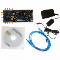
Manufacturer Part Number
AD9516-4/PCBZ
Description
BOARD EVAL FOR AD9516-4 1.8GHZ
Manufacturer
Analog Devices Inc
Specifications of AD9516-4/PCBZ
Main Purpose
Timing, Clock Generator
Embedded
No
Utilized Ic / Part
AD9516-4
Primary Attributes
2 Inputs, 14 Outputs, 1.6GHz VCO
Secondary Attributes
CMOS, LVDS, LVPECL Output Logic, ADIsimCLK™ Graphical User Interface
Silicon Manufacturer
Analog Devices
Application Sub Type
PLL Clock Synthesizer
Kit Application Type
Clock & Timing
Silicon Core Number
AD9516-0, AD9516-1, AD9516-2
Silicon Family Name
AD9516-X
Rohs Compliant
Yes
Lead Free Status / RoHS Status
Lead free / RoHS Compliant


Reg.
Addr.
(Hex)
0x143
Table 58. LVPECL Channel Dividers
Reg.
Addr.
(Hex)
0x190
0x191
0x192
0x193
0x194
Bits
[2:1]
0
Bits
[7:4]
[3:0]
7
6
5
4
[3:0]
1
0
[7:4]
[3:0]
7
6
5
Name
Divider 0 low cycles
Divider 0 high cycles
Divider 0 bypass
Divider 0 nosync
Divider 0 force high
Divider 0 start high
Divider 0 phase offset
Divider 0 direct to output
Divider 0 DCCOFF
Divider 1 low cycles
Divider 1 high cycles
Divider 1 bypass
Divider 1 nosync
Divider 1 force high
Name
OUT9 LVDS output current
OUT9 power-down
2
0
0
1
1
0: power on (default).
1: power off.
Number of clock cycles (minus 1) of the divider input during which divider output stays low.
A value of 0x0 means that the divider is low for one input clock cycle (default = 0x0).
Number of clock cycles (minus 1) of the divider input during which divider output stays high.
A value of 0x0 means that the divider is high for one input clock cycle (default = 0x0).
0: uses divider.
1: bypasses divider (default).
Nosync.
0: obeys chip-level SYNC signal (default).
1: ignores chip-level SYNC signal.
Forces divider output to high. This requires that nosync (Bit 6) also be set.
0: divider output forced to low (default).
1: divider output forced to high.
Selects clock output to start high or start low.
0: starts low (default).
1: starts high.
Phase offset (default = 0x0).
0: OUT0 and OUT1 are connected to Divider 0 (default).
1: If Register 0x1E1[1:0] = 10b, the VCO is routed directly to OUT0 and OUT1.
If Register 0x1E1[1:0] = 00b, the CLK is routed directly to OUT0 and OUT1.
If Register 0x1E1[1:0] = 01b, there is no effect.
Duty-cycle correction function.
0: enables duty-cycle correction (default).
1: disables duty-cycle correction.
Number of clock cycles of the divider input during which divider output stays low.
A value of 0x0 means that the divider is low for one input clock cycle (default = 0x0).
Number of clock cycles (minus 1) of the divider input during which divider output stays high.
A value of 0x0 means that the divider is high for one input clock cycle (default = 0x0).
0: uses divider (default).
1: bypasses divider.
Nosync.
0: obeys chip-level SYNC signal (default).
1: ignores chip-level SYNC signal.
Forces divider output to high. This requires that nosync (Bit 6) also be set.
0: divider output forced to low (default).
1: divider output forced to high.
Description
Sets output current level in LVDS mode. This has no effect in CMOS mode.
Power-down output (LVDS/CMOS).
Description
Bypasses and powers down the divider; routes input to divider output.
Connect OUT0 and OUT1 to Divider 0 or directly to VCO or CLK.
Bypasses and powers down the divider; routes input to divider output.
1
0
1
0
1
Current (mA)
1.75
3.5
5.25
7
Rev. A | Page 73 of 80
Recommended Termination (Ω)
100
100 (default)
50
50
AD9516-4
Related parts for AD9516-4/PCBZ
Image
Part Number
Description
Manufacturer
Datasheet
Request
R

Part Number:
Description:
IC CLOCK PLL/VCO 2GHZ 64LFCSP
Manufacturer:
Analog Devices Inc
Datasheet:
Part Number:
Description:
IC CLOCK GEN 2.8GHZ VCO 64-LFCSP
Manufacturer:
Analog Devices Inc
Datasheet:
Part Number:
Description:
IC,Fourteen Distributed-Output Clock Driver,LLCC,64PIN,PLASTIC
Manufacturer:
Analog Devices Inc
Datasheet:
Part Number:
Description:
IC,Ten Distributed-Output Clock Driver,LLCC,64PIN,PLASTIC
Manufacturer:
Analog Devices Inc
Datasheet:
Part Number:
Description:
IC,Ten Distributed-Output Clock Driver,LLCC,64PIN,PLASTIC
Manufacturer:
Analog Devices Inc
Datasheet:
Part Number:
Description:
Clock IC With 1.8GHz On-chip VCO
Manufacturer:
Analog Devices Inc
Datasheet:

Part Number:
Description:
BOARD EVAL FOR AD9516-2 2.2GHZ
Manufacturer:
Analog Devices Inc
Datasheet:

Part Number:
Description:
Clock IC With 2.5GHz On-chip VCO EB
Manufacturer:
Analog Devices Inc
Datasheet:
Part Number:
Description:
IC CLOCK GEN 2.8GHZ VCO 64-LFCSP
Manufacturer:
Analog Devices Inc
Datasheet:
Part Number:
Description:
IC,Ten Distributed-Output Clock Driver,LLCC,64PIN,PLASTIC
Manufacturer:
Analog Devices Inc
Datasheet:
Part Number:
Description:
IC,Fourteen Distributed-Output Clock Driver,LLCC,64PIN,PLASTIC
Manufacturer:
Analog Devices Inc
Datasheet:
Part Number:
Description:
IC,Ten Distributed-Output Clock Driver,LLCC,64PIN,PLASTIC
Manufacturer:
Analog Devices Inc
Datasheet:
Part Number:
Description:
Clock IC With 1.8GHz On-chip VCO
Manufacturer:
Analog Devices Inc
Datasheet:
Part Number:
Description:
10/14 Chan Clock IC W/PLL-no VCO
Manufacturer:
Analog Devices Inc
Datasheet:
Part Number:
Description:
10/14 Chan Clock IC W/PLL-no VCO
Manufacturer:
Analog Devices Inc
Datasheet: